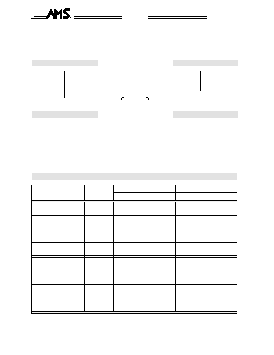
DL82 is a transparent D-latch with 2x drive strength. The Q output follows the D input
when GN is low. The Q output is independent of D when GN is high and retains the
value of D just prior to the rising edge on GN.
Truth Table
D
GN
Q
QN
Capacitance
D
GN
Q
QN
Ci (pF)
L
L
L
H
D
0.013
H
L
H
L
GN
0.023
X
H
no change
Area
Power
0.95 mils
2
4.61 µW
/
MHz
Delay [ns] = tpd.. = f(SL, L)
with SL = Input Slope [ns] ; L = Output Load [pF]
Output Slope [ns] = op_sl.. = f(L)
with L = Output Load [pF]
AC Characteristics : Tj = 25∞C VDD = 3.3V Typical Process
AC Characteristics
Characteristics
Symbol
SL = 0.1
SL = 2.0
L = 0.2
L = 1.4
L = 2.0
L = 0.2
L = 1.4
L = 2.0
Delay D to Q
tpddqr
1.02
2.48
3.19
1.11
2.57
3.26
tpddqf
1.27
2.59
3.16
1.45
2.76
3.33
Delay D to QN
tpddqnr
1.72
3.10
3.75
1.89
3.27
3.91
tpddqnf
1.47
2.62
3.17
1.57
2.71
3.26
Delay GN to Q
tpdgnqr
1.25
2.71
3.41
1.55
3.01
3.71
tpdgnqf
1.57
2.89
3.46
1.86
3.19
3.76
Delay GN to QN
tpdgnqnr
2.04
3.43
4.13
2.34
3.72
4.44
tpdgnqnf
1.71
2.86
3.45
2.02
3.17
3.73
Output Slope D to Q
op_sldqr
1.07
5.30
7.32
1.08
5.27
7.28
op_sldqf
1.01
4.05
5.30
1.00
4.02
5.32
Output Slope D to QN
op_sldqnr
1.01
5.13
7.25
0.96
5.18
7.20
op_sldqnf
0.78
3.78
5.45
0.78
3.77
5.41
Output Slope GN to Q
op_slgnqr
1.03
5.13
7.50
1.05
5.28
7.33
op_slgnqf
0.98
4.01
5.32
1.00
3.98
5.73
Output Slope GN to QN
op_slgnqnr
1.00
5.15
7.25
1.00
5.11
7.38
op_slgnqnf
0.76
3.81
5.42
0.75
3.80
5.50
Sept. 1996
- 140 -
Rev. N/C
Austria Mikro S ysteme International
R
0.6 µm CMOS
CUB
DL82
DL82
