 | –≠–ª–µ–∫—Ç—Ä–æ–Ω–Ω—ã–π –∫–æ–º–ø–æ–Ω–µ–Ω—Ç: FLASH6-C3 | –°–∫–∞—á–∞—Ç—å:  PDF PDF  ZIP ZIP |
Revision B, 07.09.02
Page 1 of 9
ANALOG IP BLOCK
FLASH6 - CMOS 6-Bit FLASH A/D CONVERTER
DATA SHEET
FEATURES
!
Small Area < 0.257 mm
2
!
Size x= 361
µm y= 710 µm
!
Supply Voltage 3.0-3.6 V
!
Junction Temp. Range -40 - 125∞C
!
Resolution 6-Bit
!
Maximum Sampling Rate 100MS/s
!
Low Input Capacitance < 5pF
!
Output Code Binary
DESCRIPTION
The FLASH6 is a complete analog to digital converter
cell which operates from a single supply. It performs
sampling, analog-to-digital conversion, generating a
6 bit value in parallel form. The output word rate can be
up to 100MS/s. The output data format is compatible
with most
µP and digital signal processors.
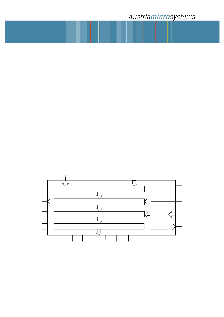
C o m p a ra t o rs
E rro r C o rre c tio n /R O M /O u tp u t L a tc h
T im in g
6 B it B u s
C L K
V D D A
V S S A
V D D
V S S
V R E F P
V R E F N
D A T A < 0 > D A T A < 1 > D A T A < 2 > D A T A < 3 > D A T A < 4 > D A T A < 5 >
V IN
R e s is to r L a d d e r
P D
S T R O B E
IB IA S
O V L
PROCESS
C35B3 (0.35um)
Data Sheet : FLASH6 - C35
Revision B, 07.09.02
Page 2 of 9
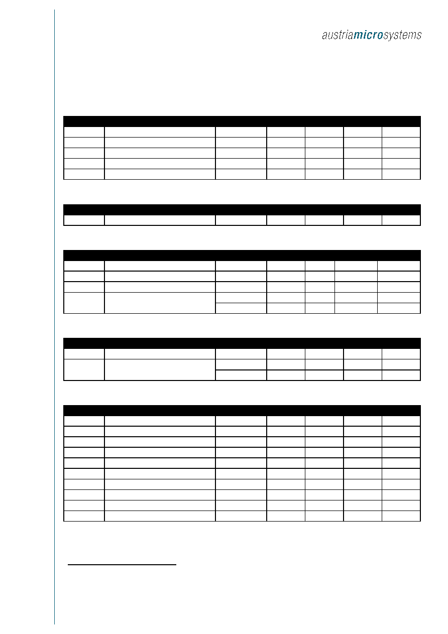
TECHNICAL DATA
(T
junction
= -40 to 125 ∞C, VDDA=VDD=+3.0V to +3.6V, fclk = 100MHz, VREFP and VREFN as specified, pad resistors as specified in the
functional block diagram, unless otherwise specified)
DC ACCURACY
Symbol
Parameter
Conditions
Min
Typ
Max
Units
Resolution (No missing Code)
6
6
6
Bit
DNL
Differential Linearity Error
-0.8
±0.4
+0.8
LSB
INL
Integral Linearity Error
-0.8
±0.4
+0.8
LSB
OFF
Offset Error
-2
+2
LSB
GAINERR
Gain Error
-2
+2
LSB
CHARACTERISTICS
Symbol
Parameter
Conditions
Min
Typ
Max
Units
IBIAS
Bias sink current
30
uA
REFERENCE CHARACTERISTICS
Symbol
Parameter
Conditions
Min
Typ
Max
Units
VREFP
Pos. Reference Voltage
1.8
2.4
2.8
V
VREFN
Neg. Reference Voltage
0.35
0.4
0.6
V
VREF
Difference between VRP and VRN
VREFP-VREFN
1.2
2
2.45
V
R
ref
Reference Impedance
1)
380
Ohm
TKR
ref
1.2
mOhm/K
ANALOG INPUT
Symbol
Parameter
Conditions
Min
Typ
Max
Units
Vin
Input Voltage Range
VREFN
VREFP
V
R
in
Input Impedance
100
MOhms
C
in
5
pF
AC ACCURACY
(VREFP=2.4V, VREFN=0.4V)
Symbol
Parameter
Conditions
Min
Typ
Max
Units
THD
Total Harmonic Distortion
f
in
=1MHz
-41.3
dB
THD
Total Harmonic Distortion
f
in
=30MHz
-41.3
dB
SFDR
Spurious Free Dynamic Range
f
in
=1MHz
46.2
dB
SFDR
Spurious Free Dynamic Range
f
in
=30MHz
46.2
dB
SNR
Signal to Noise Ratio
f
in
=1MHz
35.88
dB
SNR
Signal to Noise Ratio
f
in
=30MHz
34.1
dB
SINAD
Signal to (Noise+Dist.) Ratio
f
in
=1MHz
34.8
dB
SINAD
Signal to (Noise+Dist.) Ratio
f
in
=30MHz
33.3
dB
ENOB
Effective Number of Bits
f
in
=1MHz
5.5
Bit
ENOB
Effective Number of Bits
f
in
=30MHz
5.24
Bit
1) VREFP to VREFN
Data Sheet : FLASH6 - C35
Revision B, 07.09.02
Page 3 of 9
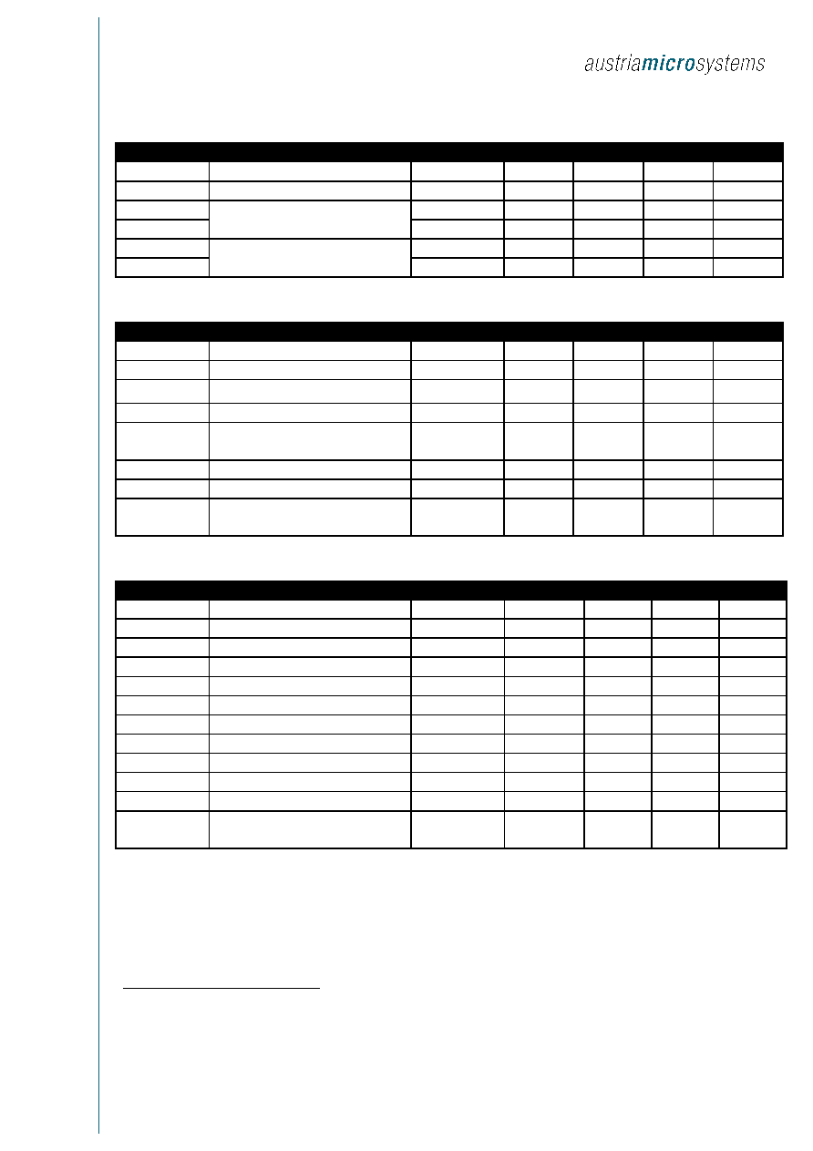
DIGITAL INPUTS AND OUTPUTS
Symbol
Parameter
Conditions
Min
Typ
Max
Units
VDD
Pos. digital Supply Voltage
VDD=VDDA
3.0
3.3
3.6
V
VSS
Neg. digital Supply Voltage
VSS=VSSA
0
0
0
V
VIL
Digital Input Level
VSS
0.3*VDD
V
VIH
0.7*VDD
VDD
V
VOL
Digital Output Level
VSS
V
VOH
VDD
V
POWER REQUIREMENTS
Symbol
Parameter
Conditions
Min
Typ
Max
Units
VDDA
Pos. analog Supply Voltage
VDD=VDDA
3.0
3.3
3.6
V
VSSA
Neg. analog Supply Voltage
VSS=VSSA
0
0
0
V
IDD
1)
3)
Supply Current Digital
7.5
15
m
IDDA
1) 3)
Supply Current Analog
4
8
mA
Psup
1) 3)
Supply Power Consumption Power Up
Mode
38
82,8
mW
IREF
1) 3)
Reference Current
incl. Ref.
5
10
mA
Pdiss_tot
1) 3)
Total Power Consumption
54,5
118,8
mW
Pdiss_pd
2) 3)
Total Power Consumption
Power Down Mode
30
60
mW
TIMING CHARACTERISTICS
Symbol
Parameter
Conditions
Min
Typ
Max
Units
1/Tconv
Conversion Rate
0.1
80
100
MS/sec
fclk
Master CLOCK Frequency
0.1
80
100
MHz
Tdap
Aperture Delay
1.8
ns
Tconv
Total Conversion Time
1
clk cycle
Tpwhclk
CLOCK Pulse width High
5
6.5
nsec
Tpwlclk
CLOCK Pulse width Low
5
6.5
nsec
Jclk
CLOCK Jitter
1*e
-3
/fin
sec
Tdcs
Delay Time CLOCK to STROBE
5.5
nsec
Tsuds
Setup Time DATA to STROBE
0.8
nsec
Tdp
Delay Time Pipeline
1
nsec
Twakeupall
Wake up Time all
50
nsec
Twakeup
Wake up Time
Twkupall -
Tdap
nsec
1)
Measured during a conversion with 100MHz clock frequency.
2)
After 10
µs power down.
3)
The measurement includes 8 digital (8mA) output pads.

Data Sheet : FLASH6 - C35
Revision B, 07.09.02
Page 4 of 9
CODE TABLE
1LSB = (VREFP - VREFN) / 64.
Output Code
Input Voltage: VIN-VINB
00 0000
VREFN.....0.5LSB
00 0001
0.5LSB.....1.5LSB
00 0010
1.5LSB.....2.5LSB
...
...
11 1111
62.5LSB.....VREFP
Data Sheet : FLASH6 - C35
Revision B, 07.09.02
Page 5 of 9
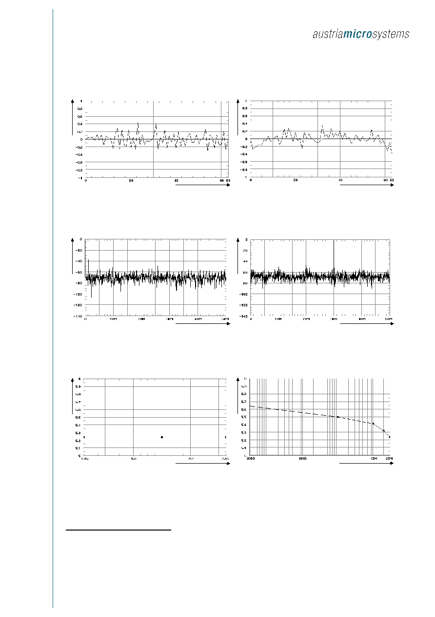
TYPICAL PERFORMANCE CHARACTERISTICS
(T
junction
=25∞C, VDDA=VDD=+3.3V, fclk=100MHz, VREFP=+2.4V and VREFN=0.4V, unless otherwise specified)
Digital Code
DNL [LSB]
Digital Code
INL [LSB]
DNL
INL
Input Signal Frequency [Hz]
FFT [dBc]
Input Signal Frequency [Hz]
FFT [dBc]
Spectrum @1MHz
1)
Spectrum @30MHz
1)
VREFP-VREFN [V]
ENOB [Bit]
pg
Input Signal Frequency [Hz]
ENOB [Bit]
ENOB vs (VREFP-VREFN) @30MHz
ENOB vs Input Signal Frequency
1)
The spectrum consists of 1024 pins
Data Sheet : FLASH6 - C35
Revision B, 07.09.02
Page 6 of 9
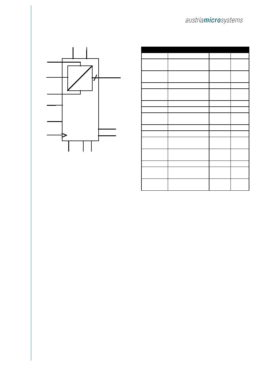
SYMBOL
PD
STROBE
FLASH6
DATA<5:0>
6
OVL
CLK
VIN
VREFP
VREFN
A
D
VDDA
VDD
VSSA
VSS
IBIAS
SHIELD
PINLIST
Pin
Description
Typ
Cap
VIN
Input Voltage
AIN
5pF
VREFP
Pos. Reference
Voltage
AIN
VREFN
Neg. Reference
Voltage
AIN
IBIAS
Bias Current
AIN
PD
Power down
Signal
DIN
0.1pF
CLK
Master Clock
DIN
0.1pF
DATA<5:0>
Data Output
(DATA<5>=MSB)
DOUT
OVL
Overload
DOUT
STROBE
Data Strobe Signal
DOUT
VDDA
Pos. Analog
Supply
S
VSSA
Neg. Analog
Supply
S
SHIELD
Connect to VSSA
S
VDD
Pos. Digital
Supply
S
VSS
Neg. Digital
Supply
S
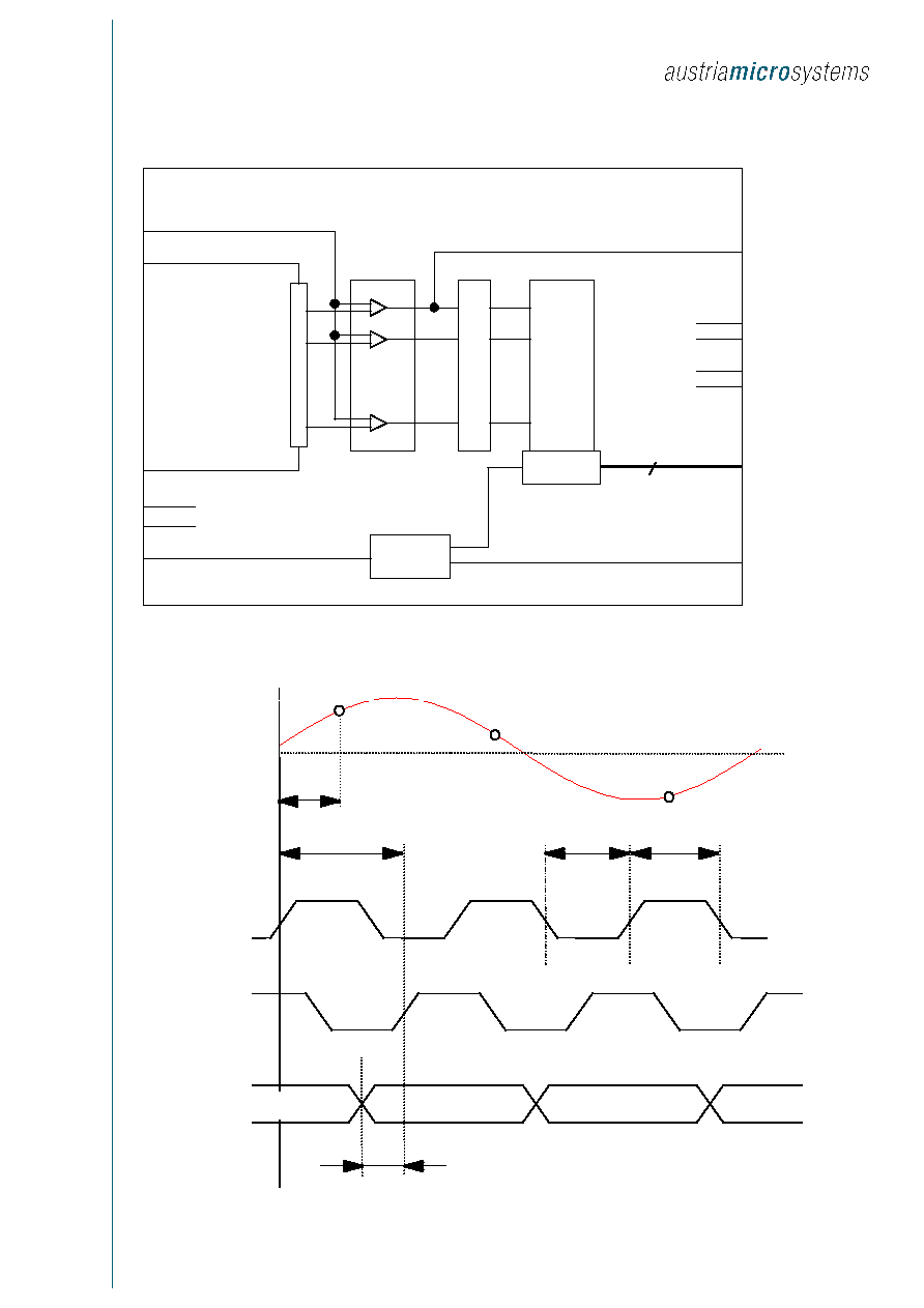
THEORY OF OPERATION
The Macro Cell FLASH6 is a 6-bit single step parallel analog to
digital converter. The architecture is based on a 380 Ohm
polysilicon resistor reference ladder and static CMOS comparators.
The thermometer code of the comparator outputs is encoded in a
fast ROM encoder into straight binary code with CMOS logic signal
levels. The last comparator output is connected unlatched to the
OVL output. The area of the converter is small. The comparators do
not need auto zeroing and therefore are fast and perform minimal
kickback on the analog signal input. The conversion range is set by
the reference inputs VREFP and VREFN. The output OVL indicates
an overload condition when Vin > (VREFP - 0.5*LSB).
POWER SUPPLIES
The converter requires a single +3.3V power supply. The supplies
for analog and digital are separated and may be connected
together. However, for maximum noise immunity it is
recommended to wire them on chip to separated pins, especially
when the block is embedded in a large digital circuit. The supplies
may then be connected together on PC-board level.
The proper use of blocking capacitors in the application is important
REFERENCE VOLTAGE
Both input pads VREFP and VREFN must have a 0 Ohm protection
resistor. The ESD test was performed with
±1kV (Norm: MIL 883 E
method 3015).
The proper use of blocking capacitors in the application is
important !
INPUT VOLTAGE
The input pad VIN must have a 0 Ohm protection resistor. The ESD
test was performed with
±1kV (Norm: MIL 883 E method 3015).
Data Sheet : FLASH6 - C35
Revision B, 07.09.02
Page 7 of 9
FUNCTIONAL BLOCK DIAGRAM
FLASH6
DATA<5:0>
CLK
PD
IBIAS
6
TIMING
LATCH
VIN
VREFP
VDDA
VSSA
VDD
VSS
Rref
E
R
R
O
R
C
O
R
R.
ROM
.
.
.
.
.
.
.
.
.
VREFN
OVL
STR
TIMING DIAGRAM OF FLASH6
Vin
CLK
STROBE
DATA<0:5>
Sample N-2
Sample N-1
Sample N
Sample N
Sample N+1
Sample N+2
Tdap
Tdcs
Tpwlclk
Tpwhclk
Tsuds

Data Sheet : FLASH6 - C35
Revision B, 07.09.02
Page 8 of 9
TYPICAL APPLICATION
VIN
10uF
VSSA
100nF
15nF
1.2nF
0.47pF
VDDA
+3.3V
0.22pF
10uF
100nF
15nF
1.2nF
0.47pF
VSS
VDD
+3.3V
0.22pF
1)
2)
1)
1)
1)
1)
2.5nF
0.3nF
0.1nF
50pF
30pF
1)
2.5nF
0.3nF
1)
0.1nF
1)
50pF
1)
30pF
1)
GROUND
A
D
VREFN
VREFP
VDDA
VDD
SHIELD
VSSA
VSS
FLASH6
OVL
STROBE
CLK
PD
IBIAS
VIN
DATA<5:0>
6
3)
Configuration: Continuous Conversion at 100MS/sec
3)
63pF
1)
30uA
100MHz
2.4V
2)
0.4V
1.4V
+3.3V
+3.3V
1)
1) The value of the capacitor depends on the input frequency.
For SMD capacitors use the type NPO and for normal capacitors use the type MKT for best performance.
2) The accuracy for both reference voltages must be higher than the resolution of the ADC. In the typical application
both voltages are filtered by a second order low pass filter (f
c
=5Hz) and buffered with an AD711.
3) The accuracy for the input voltage must be higher than the resolution of the ADC. In the typical application
the input voltage is filtered by a seven order low pass filter (f
c
=32MHz) and buffered with a THS3001.

Data Sheet : FLASH6 - C35
Revision B, 07.09.02
Page 9 of 9
Contact
austriamicrosystems AG
A 8141 Schloss Premst‰tten, Austria
T. +43 (0) 3136 500 5333
F. +43 (0) 3136 500 5755
support@austriamicrosystems.com
Copyright
Copyright © 2002 austriamicrosystems. Trademarks registered Æ.
All rights reserved. The material herein may not be reproduced,
adapted, merged, translated, stored, or used without the prior
written consent of the copyright owner. To the best of its
knowledge, austriamicrosystems asserts that the information
contained in this publication is accurate and correct.