 | –≠–ª–µ–∫—Ç—Ä–æ–Ω–Ω—ã–π –∫–æ–º–ø–æ–Ω–µ–Ω—Ç: PECL_RX | –°–∫–∞—á–∞—Ç—å:  PDF PDF  ZIP ZIP |
Revision B, 10.09.02
Page 1 of 6
ANALOG IP BLOCK
PECL_RX - CMOS PECL Receiver
DATA SHEET
FEATURES
!
PECL_RX area: 0.1
mm
2
,
size: x
= 300 µm y = 340 µm
!
PERXBIAS
size: x
= 382 µm y = 375 µm
!
3.3
V ±10% supply voltage
!
622
Mb/s transmission speed
!
1
ns max. propagation delay
!
Power dissipation 23
mW at 3.3 V static without
PERXBIAS
!
Junction temperature ≠40
- 125∞C
!
Output levels fully compatible with F100K PECL
Family
!
Power down mode
DESCRIPTION
The PECL_RX is a 3.3
V PECL differential line receiver
featuring an operating frequency up to 311
MHz (622 Mb/s)
and accepting standard F100K levels (referred to the positive
supply).
The PECL_RX accepts (750
mV) differential input signals and
translates them to CMOS output levels.
With the companion line driver (PECL_TX ) it can be used for
high speed applications.
The cell PECL_RX requires the PERXBIAS cell for biasing.
PERXBIAS can drive up to 3 PECL_RX cells. An external
voltage reference must be used.
The PECL_RX can be set in power down mode.
PROCESS
C35B3 (0.35um)

Datasheet: PECL_RX - C35
Revision B, 10.09.02
Page 2 of 6
TECHNICAL DATA FOR PECL_RX
(T
junction
= -40 to 125 ∞C, VDDPECL = VDDCMOS = VDDA = +3.0 V to +3.6 V, XPD = High, SIM = Low, unless otherwise specified)
DC CHARACTERISTICS
Symbol
Parameter
Conditions
Min
Typ
Max
Units
V
ID
Differential Input
V
ID
=
|
VINP
≠ VINN
|
250
750
900
mV
V
ICM
Common Mode Input Voltage
V
ICM
= (VINP + VINN) / 2
Referred to VDDPECL
≠1.5
-1.3
-1.1
V
V
IH
Input Voltage High
Referred to VDDPECL
≠1.165
≠0.870
V
V
IL
Input Voltage Low
Referred to VDDPECL
≠1.830
≠1.475
V
V
HYS
Hysteresis
25
100
mV
V
OH
Output Voltage High
V
V
OL
Output Voltage Low
CMOS levels
V
AC CHARACTERISTICS
C
L
= 1 pF at each output, unless otherwise specified
Symbol
Parameter
Conditions
Min
Typ
Max
Unit
t
PD
Propagation Delay
1)
600
800
1000
ps
t
SKD1
Differential Pulse Skew
1)
80
ps
t
SKD2
Differential Channel to Channel Skew
1)
100
ps
t
TLH
Rise Time
2)
150
300
600
ps
t
THL
Fall Time
2)
150
300
600
ps
C
load
Load Capacitance
@622
Mb/s
1
pF
C
in
Input Capacitance
700
900
fF
f
MAX
Operating Frequency
311
311
MHz
T
XS
Transmission Rate
622
622
Mb/s
POWER REQUIREMENTS
Symbol
Parameter
Conditions
Min
Typ
Max
Unit
I
CCDC
DC Current Consumption
Without PERXBIAS
7
10
mA
I
CCAC
AC Current Consumption
C
load
= 1 pF @622 Mb/s,
without PERXBIAS
11
15
mA
I
CCPD
Power Down Current Consumption
XPD
= Low, without
PERXBIAS
300
µ A
P
diss_DC
DC Power Consumption
Without PERXBIAS
23
36
mW
P
diss_AC
AC Power Consumption
C
load
= 1 pF @622 Mb/s,
without PERXBIAS
36
54
mW
P
diss_PD
Power Consumption in Power
Down Mode
XPD
= Low, without
PERXBIAS
1.08
mW
1)
Including the package: SOIC28, pins 5≠10 or 19≠24 for VOUTP and VOUTN
2)
Specified at 20% and 80% of the output voltage
Datasheet: PECL_RX - C35
Revision B, 10.09.02
Page 3 of 6
TECHNICAL DATA FOR PERXBIAS
(T
junction
= -40 to 125 ∞C, VDDA = +3.0 V to +3.6 V, XSIM = High, unless otherwise specified)
POWER REQUIREMENTS
Symbol
Parameter
Conditions
Min
Typ
Max
Unit
I
CC
DC Current Consumption
1.2
2
mA
P
diss
Power Consumption
4
7.2
mW
REFERENCE CHARACTERISTICS
Symbol
Parameter
Conditions
Min
Typ
Max
Unit
VREF
Reference Voltage
1.20
1.22
1.24
V

Datasheet: PECL_RX - C35
Revision B, 10.09.02
Page 4 of 6
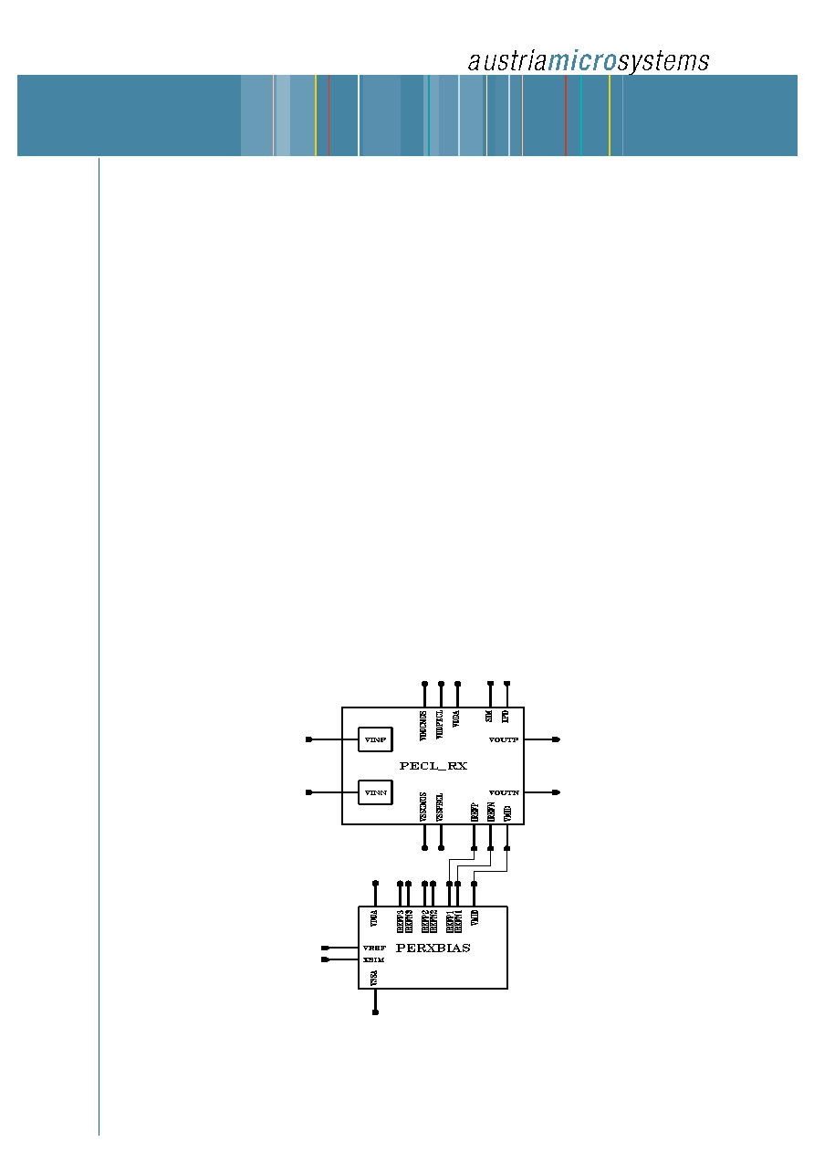
SYMBOL OF PECL_RX
XPD
VINP
VINN
VOUTP
VOUTN
High
High
Low
High
Low
High
Low
High
Low
High
Low
X
X
High
Low
PIN LIST OF PECL_RX
Pin
Description
Type
VDDPECL
Positive Supply for PECL
Receiver
Supply
VDDA
Positive Supply
Supply
VDDCMOS
Positive Supply for CMOS
Output Buffer
Supply
VSSPECL
Negative Supply
Supply
VSSCMOS
Negative Supply
Supply
IREFP
Bias Current
Analog
IREFN
Bias Current
Analog
VMID
Voltage Reference
Analog
XPD
Power Down
Digital
SIM
Test Pin
Digital
VINP
Positive Input
Analog
VINN
Negative Input
Analog
VOUTP
Pos. PECL Output
Digital
VOUTN
Neg. PECL Output
Digital
SYMBOL OF PERXBIAS
PIN LIST OF PERXBIAS
Pin
Description
Type
VDDA
Positive Supply
Supply
VSSA
Negative Supply
Supply
IREFP1
Bias Current
Analog
IREFP2
Bias Current
Analog
IREFP3
Bias Current
Analog
IREFN1
Bias Current
Analog
IREFN2
Bias Current
Analog
IREFN3
Bias Current
Analog
VMID
Voltage Reference
Analog
XSIM
Test Pin
Digital
VREF
External Reference
Voltage
Analog
THEORY OF OPERATION
The PECL_RX is a differential line receiver which accepts low
voltage input signals according to F100K standard.
The input signal lines must be 50
transmission lines. At the
receiver input each signal has to be terminated to the voltage level
V
T
(where V
T
= VDDPECL ≠ 2 V) with an external termination
resistor of 50
, but also other termination schemes are possible.
The cell PECL_RX can be set in power down mode. It requires the
PERXBIAS cell for biasing. PERXBIAS can drive up to 3
PECL_RX cells. An external voltage reference must be used.

Datasheet: PECL_RX - C35
Revision B, 10.09.02
Page 5 fo 6
APPLICATION
!
High Speed Backplane Driver
!
Complementary Clock Drivers
!
Level Translator
!
System Interconnects
!
ATM Applications
!
SDH Applications
!
High-Resolution Imaging Applications
!
Laser Printers
!
Digital Copiers
TYPICAL APPLICATION
1)
µF
1
µF
1
VDDA
VSSA
22pF
100pF
VREF (external reference)
2)
SNAP BACK
6)
50
3)
µF
1
22pF
100pF
VDDA
VT
-
2V
VREF
VSSA
3)
180pF
1nF
50
50
+
external
chip internal
VDD
4)
VDDA
1)
1) 4)
VDDA
SNAP BACK
6)
VSS
4)
3)
VSSA
4)
3)
7)
7)
7)
5)
complementary
CMOS signals
(to digital core)
VDD
VSS
3)
22pF
100pF
DATA
transmission lines
from transmitter
DATAN
VT
VT
1)
Each power pin must have its own set of blocking capacitors.
2)
An external reference must be used.
3)
VSSA and VSS must be connected on the PCB level.
4)
The two power pads can be bonded to one package pin (double bonding).
5)
Two more PECL_RX cells can be driven with IREFxx of the PERXBIAS cell. If an output IREFxx is not used it must be left unconnected.
6)
The PECL part of the chip has to be separated from the rest of the chip by use of snap backs (cell PWRCUT_DIG_P_SNAP_SNAP).
7)
The cells VDD3R1P and VDD3R2P are not in the standard library, they are part of the IP-block.

Datasheet: PECL_RX - C35
Revision B, 10.09.02
Page 6 fo 6
Contact
austriamicrosystems AG
A 8141 Schloss Premst‰tten, Austria
T. +43 (0) 3136 500 5333
F. +43 (0) 3136 500 5755
support@austriamicrosystems.com
Copyright
Copyright © 2002 austriamicrosystems. Trademarks registered Æ.
All rights reserved. The material herein may not be reproduced,
adapted, merged, translated, stored, or used without the prior
written consent of the copyright owner. To the best of its
knowledge, austriamicrosystems asserts that the information
contained in this publication is accurate and correct.