
AF1333P
P-Channel Enhancement Mode Power MOSFET
This datasheet contains new product information. Anachip Corp. reserves the rights to modify the product specification without notice. No liability is assumed as a result of the use of
this product. No rights under any patent accompany the sale of the product.
Rev. 1.0 Oct 15, 2004
1/5
Features
- Simple Gate Drive
- Fast Switching Speed
- Small Package Outline (SOT323)
Product Summary
BV
DSS
= -20V
R
DS (on)
= 800m.
I
D
= -550mA
Pin Assignments
3
2
1
(Top View)
1. G
2. S
3. D
Description
The advanced power MOSFET provides the designer
with the best combination of fast switching, low
on-resistance and cost-effectiveness.
Pin Descriptions
Pin
No.
Pin
Name
Description
1 G
Gate
2 S
Source
3 D
Drain
Ordering information
A X 1333P X X X
PN
Package
Feature
F :MOSFET
U: SOT323
Lead Free
Blank : Normal
L : Lead Free Package
Packing
Blank : Tube or Bulk
A : Tape & Reel
Block Diagram
S
G
D

AF1333P
P-Channel Enhancement Mode Power MOSFET
Anachip Corp.
www.anachip.com.tw Rev. 1.0 Oct 15, 2004
2/5
Absolute Maximum Ratings
Symbol
Parameter
Rating
Unit
V
DS
Drain-Source
Voltage
-20
V
V
GS
Gate-Source
Voltage
�12
V
T
A
=25�C -550
I
D
Continuous
Drain
Current
(Note 1)
T
A
=70�C -440
mA
I
DM
Pulsed Drain Current
(Note 2, 3)
-2.5
A
Total Power Dissipation
T
A
=25�C 0.35 W
P
D
Linear Derating Factor
0.003
W/
o
C
T
STG
Storage Temperature Range
-55 to +150
o
C
T
J
Operating Junction Temperature Range
-55 to +150
o
C
Thermal Data
Symbol
Parameter
Value
Unit
Rthj-a
Thermal Resistance Junction-Ambient
(Note 1)
Max.
360
�C/W
Electrical Characteristics
at T
A
=25
o
C (unless otherwise specified)
Symbol
Parameter
Test Conditions
Min.
Typ.
Max.
Unit
BV
DSS
Drain-Source
Breakdown
Voltage V
GS
=0V, I
D
=-250uA -20 - - V
BV
DSS
/
T
J
Breakdown Voltage Temperature
Coefficient
Reference to 25
o
C,
I
D
=-1mA
- 0.01 - V/
o
C
V
GS
=-10V, I
D
=-550mA
- -
600
V
GS
=-4.5V, I
D
=-550mA
- -
800
R
DS(ON)
Static Drain-Source
On-Resistance
V
GS
=-2.5V, I
D
=-300mA
- -
1000
m
V
GS(th)
Gate Threshold Voltage
V
DS
=V
GS
, I
D
=-250uA -0.5 - -1.2 V
g
fs
Forward
Transconductance V
DS
=-5V, I
D
=-500mA - 1 - S
Drain-Source Leakage Current
(T
J
=25
o
C)
V
DS
=-20V, V
GS
=0V - -
-1
I
DSS
Drain-Source Leakage Current
(T
J
=70
o
C)
V
DS
=-16V, V
GS
=0V - -
-10
uA
I
GSS
Gate-Source
Leakage
V
GS
=�12V -
-
�100
nA
Q
g
Total
Gate
Charge
(Note 3)
-
1.7
2.7
Q
gs
Gate-Source
Charge
- 0.3 -
Q
gd
Gate-Drain
("Miller")
Charge
I
D
=-500mA,
V
DS
=-16V,
V
GS
=-4.5V
- 0.4 -
nC
t
d(on)
Turn-On Delay Time
(Note 3)
-
5
-
t
r
Rise
Time
- 8 -
t
d(off)
Turn-Off Delay Time
-
10
-
t
f
Fall-Time
V
DS
=-10V,
I
D
=-500mA,
R
G
=3.3, V
GS
=-5V
R
D
=20
- 2 -
ns
C
iss
Input
Capacitance
- 66
105.6
C
oss
Output
Capacitance
- 25 -
C
rss
Reverse
Transfer
Capacitance
V
GS
=0V,
V
DS
=-10V,
f=1.0MHz
- 20 -
pF
Source-Drain Diode
Symbol
Parameter
Test Conditions
Min.
Typ.
Max.
Unit
V
DS
Forward On Voltage
(Note 3)
I
S
=-300mA, V
GS
=0V - -
-1.2
V
Note 1: Surface mounted on FR4 board, t 10 sec.
Note 2: Pulse width limited by Max. junction temperature.
Note 3: Pulse width 300us, duty cycle 2%.
AF1333P
P-Channel Enhancement Mode Power MOSFET
Anachip Corp.
www.anachip.com.tw Rev. 1.0 Oct 15, 2004
3/5
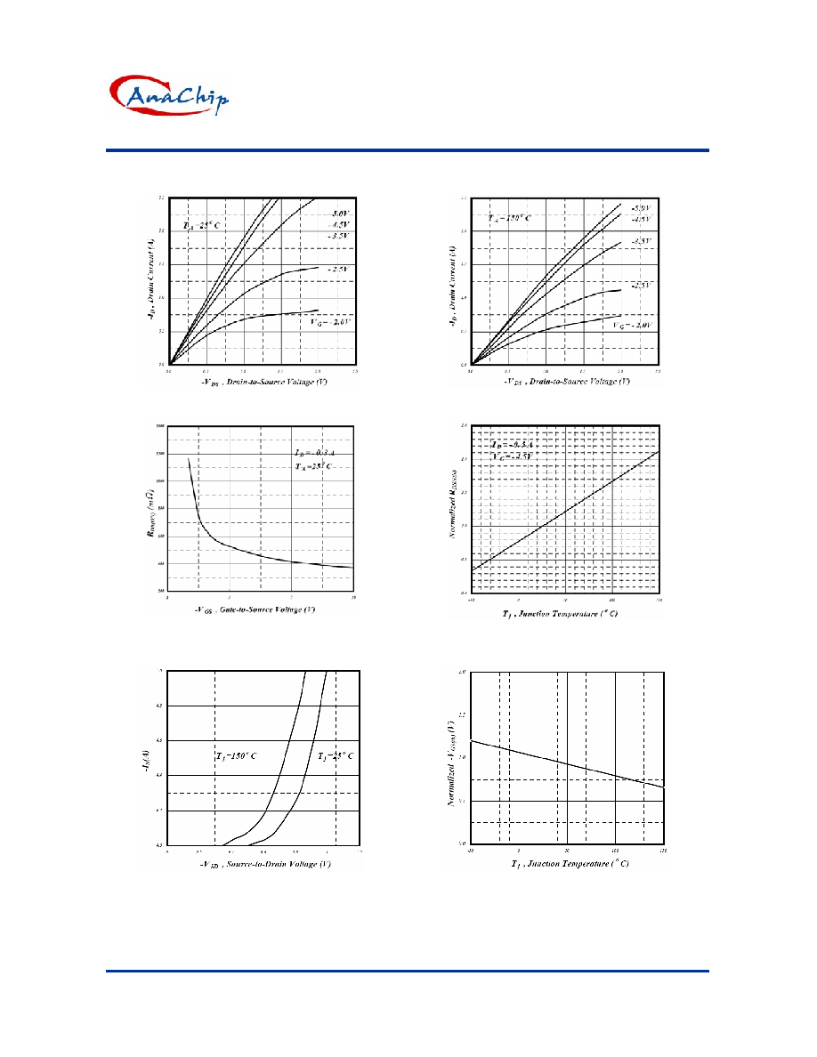
Typical Performance Characteristics
Fig 1. Typical Output Characteristics
Fig 2. Typical Output Characteristics
Fig 3. On-Resistance v.s. Gate Voltage
Fig 4. Normalized On-Resistance v.s. Junction
Temperature
Fig 5. Forward Characteristic of Reverse Diode
Fig 6. Gate Threshold Voltage v.s. Junction
Temperature
AF1333P
P-Channel Enhancement Mode Power MOSFET
Anachip Corp.
www.anachip.com.tw Rev. 1.0 Oct 15, 2004
4/5
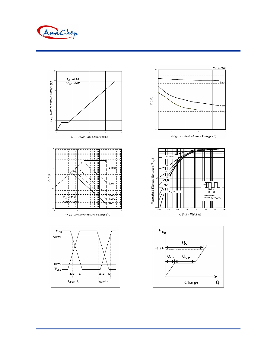
Typical Performance Characteristics (Continued)
Fig 7. Gate Charge Characteristics
Fig 8. Typical capacitance Characteristics
Fig 9. Maximum Safe Operating Area
Fig 10. Effective Transient Thermal Impedance
Fig 11. Switching Time Waveform
Fig 12. Gate Charge Waveform
AF1333P
P-Channel Enhancement Mode Power MOSFET
Anachip Corp.
www.anachip.com.tw Rev. 1.0 Oct 15, 2004
5/5
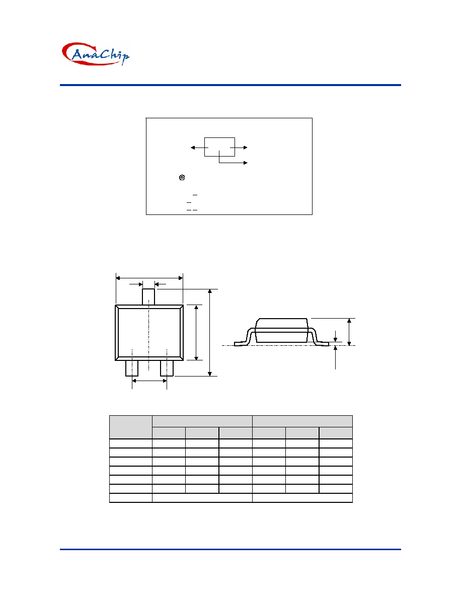
Marking Information
3 X X
SOT323
(Top View)
Part Number:
AF1333P
A~Z: Week: 27~52
or Lot No: 1~9
A~Z: Week: 01~26
or Lot No: 1~9
X X: Year: 4 years in one cycle
X X: 2004, 2008, 2012...
X X: 2005, 2009, 2013...
X X: 2006, 2010, 2014...
X X: 2007, 2011, 2015...
Package Information
Package Type: SOT323
e
E1
E
D1
D
A
A1
*Dimension does not include mold protrusions.
Dimensions In Millimeters
Dimensions In Inches
Symbol
Min.
Nom.
Max.
Min.
Nom.
Max.
A 0.90
1.00
1.10
0.035
0.039
0.043
A1 0.03
0.07
0.10
0.001
0.003
0.004
D 1.90
2.00
2.10
0.075
0.079
0.083
D1 0.20
0.30
0.40
0.008
0.012
0.016
E 2.00
2.10
2.20
0.079
0.083
0.087
E1 1.15
1.25
1.35
0.045
0.049
0.053
e
1.30 Bsc.
0.051 Bsc.