AF2302N
20V N-Channel Enhancement Mode MOSFET
This datasheet contains new product information. Anachip Corp. reserves the rights to modify the product specification without notice. No liability is assumed as a result of the use of
this product. No rights under any patent accompany the sale of the product.
Rev. 1.1 Jul 20, 2004
1/4
Features
- Advanced trench process technology
- High density cell design for ultra low on-resistance
- Excellent thermal and electrical capabilities
- Compact and low profile SOT-23 package
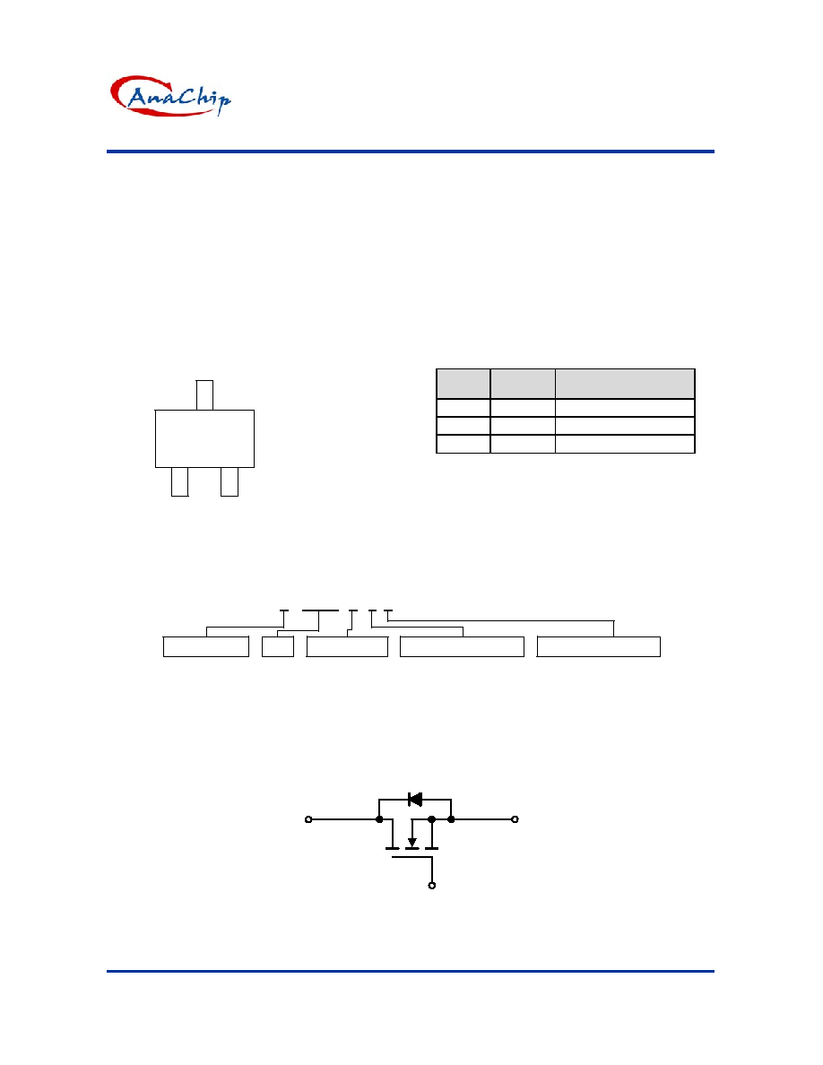
Pin Assignments
3
2
1
(Top View)
1. G
2. S
3. D
Product Summary
V
DS
= 20V
R
DS (on)
, V
GS
@4.5V, I
DS
@3.6A =65m.
R
DS (on)
, V
GS
@2.5V, I
DS
@3.1A =95m.
Pin Descriptions
Pin
No.
Pin
Name
Description
1 G
Gate
2 S
Source
3 D
Drain
Ordering information
A X 2302N X X X
PN
Package
Feature
F :MOSFET
W: SOT23
Lead Free
Blank : Normal
L : Lead Free Package
Packing
Blank : Tube or Bulk
A : Tape & Reel
Block Diagram
S
G
D
AF2302N
20V N-Channel Enhancement Mode MOSFET
Anachip Corp.
www.anachip.com.tw Rev. 1.1 Jul 20, 2004
2/4
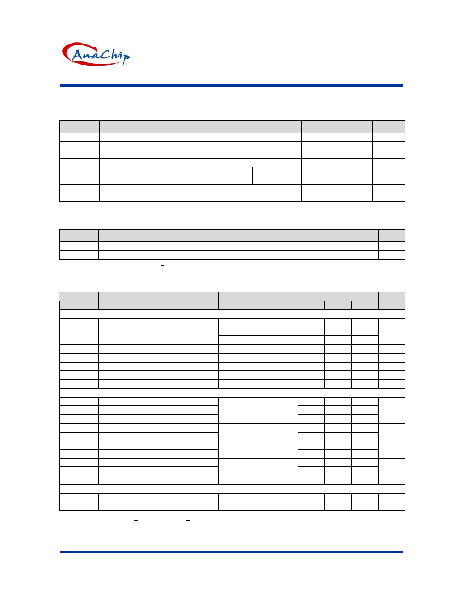
Absolute Maximum Ratings
(T
A
=25�C unless otherwise noted)
Symbol
Parameter
Rating
Units
V
DS
Drain-Source
Voltage
20
V
V
GS
Gate-Source
Voltage
�8
V
I
D
Continuous Drain Current
2.4
A
I
DM
Pulsed Drain Current
10
A
T
A
=25�C 1.25
P
D
Maximum Power Dissipation
T
A
=70�C 0.8
W
T
J
Operating
Junction
Temperature
+150
�C
T
J
, T
STG
Operating Junction and Storage Temperature Range
-55 to +150
�C
Thermal Performance
Symbol
Parameter
Limit
Units
T
L
Lead Temperature (1/8" from case)
5
S
R
JA
Junction to Ambient Thermal Resistance (PCB mounted)
100
�C/W
Note: Surface mounted on FR4 board t < 5 sec.
Electrical Characteristics
Rate I
D
=2.4A, (T
A
=25
o
C unless otherwise noted)
Limits
Symbol
Parameter
Test Conditions
Min.
Typ.
Max.
Unit
Static
BV
DSS
Drain-Source
Breakdown
Voltage V
GS
=0V, I
D
=250uA 20
-
-
V
V
GS
=4.5V, I
D
=3.6A -
50
65
R
DS(ON)
Drain-Source On-State Resistance
V
GS
=2.5V, I
D
=3.1A -
75
95
m
V
GS(TH)
Gate
Threshold
Voltage
V
DS
= V
GS
, I
D
=250uA 0.45
- - V
I
DSS
Zero Gate Voltage Drain Current
V
DS
=20V, V
GS
=0V -
-
1.0
uA
I
GSS
Gate
Body
Leakage
V
GS
=�8V, V
DS
=0V -
-
�100
nA
I
D(ON)
On-State
Drain
Current
V
DS
=5V, V
GS
=4.5V 6
-
-
A
g
fs
Forward
Tranconductance
V
DS
=5V, I
D
=3.6A -
10
-
S
Dynamic
Q
g
Total Gate Charge
-
5.2
10
Q
gs
Gate-Source
Charge
- 0.65 -
Q
gd
Gate-Drain
Charge
V
DS
=10V, I
D
=3.6A,
V
GS
=4.5V
- 1.5 -
nC
t
d(on)
Turn-On Delay Time
-
7
15
t
r
Turn-On Rise Time
-
55
80
t
d(off)
Turn-Off Delay Time
-
16
60
t
f
Turn-Off
Fall-Time
V
DD
=10V, R
L
=10,
I
D
=1A, V
GEN
=4.5V,
R
G
=6
- 10 25
nS
C
iss
Input
Capacitance
- 450 -
C
oss
Output
Capacitance
- 70 -
C
rss
Reverse Transfer Capacitance
V
DS
=10V, V
GS
=0V,
f=1.0MHz
- 43 -
pF
Source-Drain Diode
I
S
Max. Diode Forward Current
-
-
1.6
A
V
SD
Diode Forward Voltage
I
S
=1.0A, V
GS
=0V -
0.75
1.2
V
Note: Pulse test: pulse width < 300uS, duty cycle < 2%
AF2302N
20V N-Channel Enhancement Mode MOSFET
Anachip Corp.
www.anachip.com.tw Rev. 1.1 Jul 20, 2004
3/4
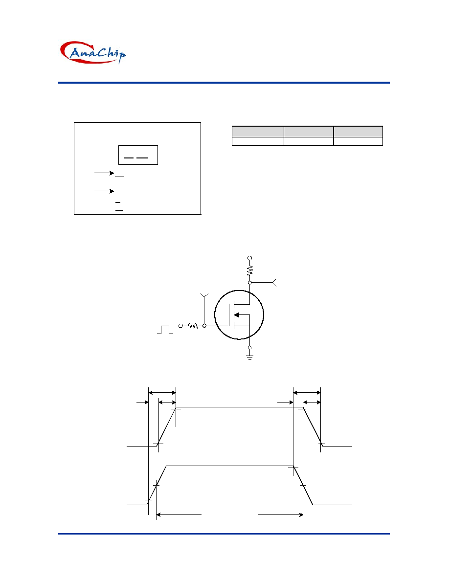
Marking Information
XX YW
SOT23
Date code
Y : Year
W : Week(A~Z)
XX: Device Code
(Top View)
(See Appendix)
Appendix
Part Number
Package
Device Code
AF2302N SOT23-3
02
Switching Test Circuit
S
G
D
V
DD
R
G
V
GEN
V
IN
V
OUT
R
D
OUT
Switching Waveforms
PULSE WIDTH
t
on
t
r
t
d(on)
90%
Output, V
OUT
10%
10%
50%
Input, V
IN
t
off
t
d(off)
t
f
90%
10%
90%
50%
INVERTED
AF2302N
20V N-Channel Enhancement Mode MOSFET
Anachip Corp.
www.anachip.com.tw Rev. 1.1 Jul 20, 2004
4/4
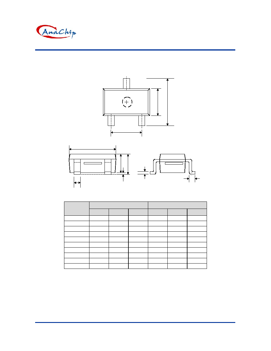
Package Information
C
L
e
E
HE
D
A2
A1
b
A
Dimensions In Millimeters
Dimensions In Inches
Symbol
Min.
Nom.
Max.
Min.
Nom.
Max.
A 1.00
1.20
1.40
0.039
0.047
0.055
A1 0.00 - 0.10
0.000 - 0.004
A2 1.00
1.15
1.30
0.039
0.045
0.051
b 0.35 - 0.50
0.014
-
0.020
C
0.10 0.175 0.25 0.004 0.007 0.010
D 2.70
2.90
3.10
0.106
0.114
0.122
E 1.40
1.60
1.80
0.055
0.063
0.071
e 1.70
2.00
2.30
0.067
0.079
0.091
HE 2.40
2.70
3.00
0.094
0.106
0.118
L 0.30 - 0.55
0.012
-
0.022