AF4407P
P-Channel 30-V (D-S) MOSFET
This datasheet contains new product information. Anachip Corp. reserves the rights to modify the product specification without notice. No liability is assumed as a result of the use of
this product. No rights under any patent accompany the sale of the product.
Rev. 1.0 Jul 16, 2004
1/5
Features
-Low r
DS(on)
Provides Higher Efficiency and Extends
Battery Life
-Miniature SO-8 Surface Mount Package Saves
Board Space
-High power and current handling capability
-Extended V
GS
range (±25) for battery pack
applications
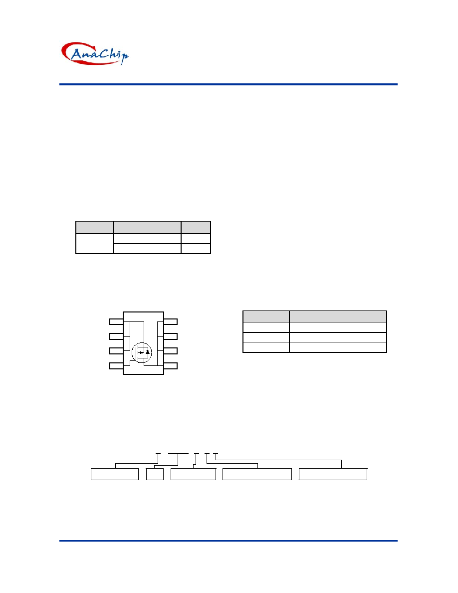
Product Summary
V
DS
(V)
r
DS(on)
(m)
I
D
(A)
9@V
GS
=-10V -15
-30
13@V
GS
=-4.5V -11
Pin Assignments
SOP-8
5
6
7
8
4
3
2
1
D
D
D
D
S
S
S
G
General Description
These miniature surface mount MOSFETs utilize
High Cell Density process. Low r
DS(on)
assures
minimal power loss and conserves energy, making
this device ideal for use in power management
circuitry. Typical applications are PWM DC-DC
converters, power management in portable and
battery-powered products such as computers,
printers, battery charger, telecommunication power
system, and telephones power system.
Pin Descriptions
Pin Name
Description
S Source
G Gate
D Drain
Ordering information
A X 4407P X X X
PN
Package
Feature
F :MOSFET
S: SOP-8
Lead Free
Blank : Normal
L : Lead Free Package
Packing
Blank : Tube or Bulk
A : Tape & Reel

AF4407P
P-Channel 30-V (D-S) MOSFET
Anachip Corp.
www.anachip.com.tw Rev. 1.0 Jul 16, 2004
2/5
Absolute Maximum Ratings
(T
A
=25∫C unless otherwise noted)
Symbol
Parameter
Rating
Units
V
DS
Drain-Source
Voltage
-30
V
V
GS
Gate-Source
Voltage
±25
V
T
A
=25∫C -15
I
D
Continuous
Drain
Current
(Note 1)
T
A
=70∫C -11
A
I
DM
Pulsed Drain Current
(Note 2)
±50
A
I
S
Continuous Source Current (Diode Conduction)
(Note 1)
-2.1
A
T
A
=25∫C 3.1
P
D
Power
Dissipation
(Note 1)
T
A
=70∫C 2.3
W
T
J
, T
STG
Operating and Storage Junction Temperature Range
-55 to 150
∫C
Thermal Resistance Ratings
Symbol
Parameter
Maximum
Units
R
JC
Maximum
Junction-to-Case
(Note 1)
t < = 5 sec
25
∫C/W
R
JA
Maximum
Junction-to-Ambient
(Note 1)
t < = 5 sec
50
∫C/W
Note 1: surface Mounted on 1"x 1" FR4 Board.
Note 2: Pulse width limited by maximum junction temperature
Specifications
(T
A
=25∫C unless otherwise noted)
Limits
Symbol
Parameter
Test Conditions
Min.
Typ.
Max.
Unit
Static
V
(BR)DSS
Drain-Source breakdown Voltage
V
GS
=0V, I
D
=-250uA -30
- - V
V
GS(th)
Gate-Threshold
Voltage
V
DS
= V
GS
, I
D
=-250uA -1
-1.6
-3 V
I
GSS
Gate-Body
Leakage
V
DS
=0V, V
GS
=±25V -
-
±100
nA
V
DS
=-24V, V
GS
=0V -
-
-1
I
DSS
Zero Gate Voltage Drain Current
V
DS
=-24V, V
GS
=0V,
T
J
=55∫C
- - -5
uA
I
D(on)
On-State
Drain
Current
(Note 3)
V
GS
=-5V, V
DS
=-10V -50 - - A
V
GS
=-10V, I
D
=-13A -
7.3
9
V
GS
=-4.5V, I
D
=-11A -
10
13
r
DS(on)
Drain-Source
On-Resistance
(Note 3)
V
GS
=-10V, I
D
=-13A,
T
J
=55∫C
- 9 11
m
g
fs
Forward
Tranconductance
(Note 3)
V
GS
=-5V, I
D
=-13A -
44
-
S
V
SD
Diode Forward Voltage
I
S
=2.1A, V
GS
=0V -
-0.7
-1.2
V
Dynamic
(Note 4)
Q
g
Total Gate Charge
-
71
100
Q
gs
Gate-Source
Charge
- 12 -
Q
gd
Gate-Drain
Charge
V
DS
=-15V, V
GS
=-10V,
I
D
=-13A
- 15 -
nC
Switching
t
d(on)
Turn-On Delay Time
-
19
36
t
r
Rise
Time
- 11 21
t
d(off)
Turn-Off Delay Time
-
121
186
t
f
Fall-Time
V
DD
=-15V, R
L
=6,
ID=-1A, VGEN=-10V
- 68
112
nS
Note 3: Pulse test: PW < 300us duty cycle < 2%.
Note 4: Guaranteed by design, not subject to production testing.

AF4407P
P-Channel 30-V (D-S) MOSFET
Anachip Corp.
www.anachip.com.tw Rev. 1.0 Jul 16, 2004
3/5
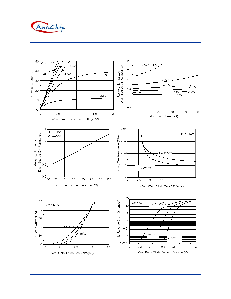
Typical Performance Characteristics
Figure 1. On-Region Characteristics
Figure 2. On-Resistance Variation with
Drain Current and Gate Voltage
Figure 3. On-Resistance Variation
With Temperature
Figure 4. On-Resistance Variation with
Gate to Source Voltage
Figure 5. Transfer Characteristics
Figure 6. Body Diode Forward Voltage Variation
With Source Current and Temperature

AF4407P
P-Channel 30-V (D-S) MOSFET
Anachip Corp.
www.anachip.com.tw Rev. 1.0 Jul 16, 2004
4/5
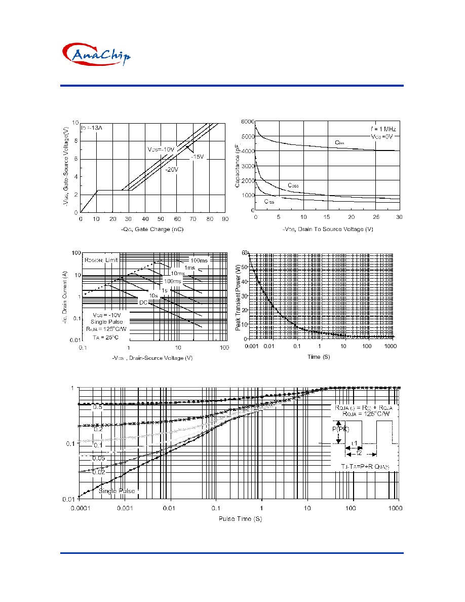
Typical Performance Characteristics (Continued)
Figure 7. Gate Charge Characteristics
Figure 8. Capacitance Characteristics
Figure 9. Maximum Safe Operating Area
Figure 10. Single Pulse Maximum Power Dissipation
Normalized Thermal Transient Junction To Ambient
Figure 11. Transient Thermal Response Curve

AF4407P
P-Channel 30-V (D-S) MOSFET
Anachip Corp.
www.anachip.com.tw Rev. 1.0 Jul 16, 2004
5/5
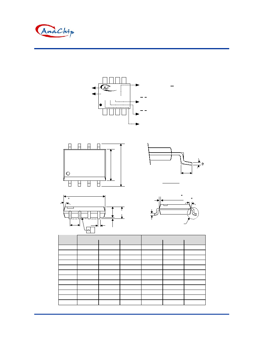
Marking Information
SOP-8L
( Top View )
1
8
4 4 0 7 P
AA Y W X
Year code:
Part Number
Lot code:
Week code:
Factory code
"A~Z": 01~26;
"A~Z": 27~52
"4" =2004
~
"A~Z": 01~26;
"A~Z": 27~52
"X": Non-Lead Free; "X": Lead Free
Logo
Package Information
Package Type: SOP-8L
VIEW "A"
L
C
VIEW "A"
H
E
A
A2
A1
B
e
D
7 (4X)
0.015x45
7 (4X)
y
Dimensions In Millimeters
Dimensions In Inches
Symbol
Min.
Nom.
Max.
Min.
Nom.
Max.
A 1.40 1.60 1.75 0.055 0.063 0.069
A1
0.10 - 0.25
0.040 - 0.100
A2 1.30 1.45 1.50 0.051 0.057 0.059
B 0.33 0.41 0.51 0.013 0.016 0.020
C 0.19 0.20 0.25 0.0075
0.008
0.010
D 4.80 5.05 5.30 0.189 0.199 0.209
E 3.70 3.90 4.10 0.146 0.154 0.161
e - 1.27 - - 0.050 -
H 5.79 5.99 6.20 0.228 0.236 0.244
L 0.38 0.71 1.27 0.015 0.028 0.050
y - - 0.10 - - 0.004
0
O
- 8
O
0
O
- 8
O
