AF4920N
N-Channel Enhancement Mode Power MOSFET
This datasheet contains new product information. Anachip Corp. reserves the rights to modify the product specification without notice. No liability is assumed as a result of the use of
this product. No rights under any patent accompany the sale of the product.
Rev. 1.0 Oct 13, 2005
1/5
Features
- Low On-resistance
- Simple Drive Requirement
- Dual N MOSFET Package
Product Summary
BV
DSS
(V)
R
DS(ON)
(m)
I
D
(A)
30 18
8.2
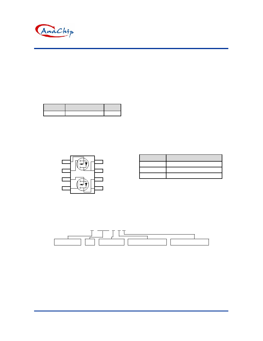
Pin Assignments
SO-8
5
6
7
8
4
3
2
1
D1
D1
D2
D2
S1
G1
S2
G2
General Description
The advanced power MOSFET provides the designer
with the best combination of fast switching,
ruggedized device design, ultra low on-resistance and
cost-effectiveness.
Pin Descriptions
Pin Name
Description
S1/2
Channel
1/2
Source
G1/2
Channel 1/2 Gate
D1/2
Channel 1/2 Drain
Ordering information
A X 4920N X X X
PN
Package
Feature
F :MOSFET
S: SO-8
Lead Free
Blank : Normal
L : Lead Free Package
Packing
Blank : Tube or Bulk
A : Tape & Reel
AF4920N
N-Channel Enhancement Mode Power MOSFET
Anachip Corp.
www.anachip.com.tw Rev. 1.0 Oct 13, 2005
2/5
Absolute Maximum Ratings
Symbol
Parameter
Rating
Units
V
DS
Drain-Source
Voltage
30
V
V
GS
Gate-Source
Voltage
�20
V
T
A
=25�C 8.2
I
D
Continuous Drain Current
(Note 1)
T
A
=70�C 6.7
A
I
DM
Pulsed
Drain
Current
(Note 2)
30
A
Total Power Dissipation
2
W
P
D
Linear Derating Factor
T
A
=25�C
0.016 W/�C
T
STG
Storage Temperature Range
-55 to 150
�C
T
J
Operating Junction Temperature Range
-55 to 150
�C
Thermal Data
Symbol
Parameter
Maximum
Units
Rthj-amb Thermal
Resistance
Junction-ambient
(Note 1)
Max.
62.5 �C/W
Electrical Characteristics
at T
J
=25�C unless otherwise specified
Symbol
Parameter
Test Conditions
Min.
Typ.
Max.
Units
BV
DSS
Drain-Source
Breakdown
Voltage V
GS
=0V, I
D
=250uA 30
- - V
BV
DSS
/
T
J
Breakdown Voltage Temperature
Coefficient
Reference to 25
o
C,
I
D
=1mA
- 0.03 - V/
o
C
V
GS
=10V, I
D
=6A -
-
18
R
DS(ON)
Static Drain-Source
On-Resistance
(Note 3)
V
GS
=4.5V, I
D
=4A -
-
28
m
V
GS(th)
Gate Threshold Voltage
V
DS
=V
GS
, I
D
=250uA 1 - 3 V
g
fs
Forward
Transconductance V
DS
=10V, I
D
=6A -
15
-
S
Drain-Source Leakage Current
(T
J
=25
o
C)
V
DS
=30V, V
GS
=0V -
-
1
I
DSS
Drain-Source Leakage Current
(T
J
=70
o
C)
V
DS
=24V, V
GS
=0V -
-
25
uA
I
GSS
Gate-Source
Leakage
V
GS
=�20V -
-
�100
nA
Q
g
Total
Gate
Charge
(Note 3)
-
23
30
Q
gs
Gate-Source
Charge
- 6 -
Q
gd
Gate-Drain
("Miller")
Charge
I
D
=8A,
V
DS
=24V,
V
GS
=4.5V
- 14 -
nC
t
d(on)
Turn-On Delay Time
(Note 3)
-
12
-
t
r
Rise
Time
- 8 -
t
d(off)
Turn-Off Delay Time
-
34
-
t
f
Fall-Time
V
DS
=15V,
I
D
=1A,
R
G
=3.3, V
GS
=10V
R
D
=15
- 16 -
ns
C
iss
Input
Capacitance
- 1450
2320
C
oss
Output
Capacitance
- 320 -
C
rss
Reverse
Transfer
Capacitance
V
GS
=0V,
V
DS
=25V,
f=1.0MHz
- 230 -
pF
R
G
Gate
Resistance
f=1.0MHz
- 0.9 -
Source-Drain Diode
Symbol
Parameter
Test Conditions
Min.
Typ.
Max.
Unit
V
SD
Forward On Voltage
(Note 3)
I
S
=1.7A, V
GS
=0V -
-
1.2
V
t
rr
Reverse
Recovery
Time
(Note 3)
- 27 - ns
Q
rr
Reverse Recovery Charge
I
S
=8A, V
GS
=0V,
dl/dt=100A/�s
- 18 - nC
Note 1: Surface mounted on 1 in
2
copper pad of FR4 board; 135
o
C/W when mounted on Min. copper pad.
Note 2: Pulse width limited by Max. junction temperature.
Note 3: Pulse width 300us, duty cycle 2%.
AF4920N
N-Channel Enhancement Mode Power MOSFET
Anachip Corp.
www.anachip.com.tw Rev. 1.0 Oct 13, 2005
3/5
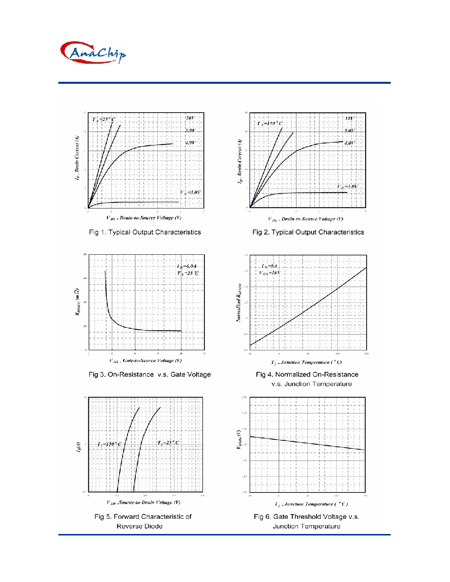
Typical Performance Characteristics
AF4920N
N-Channel Enhancement Mode Power MOSFET
Anachip Corp.
www.anachip.com.tw Rev. 1.0 Oct 13, 2005
4/5
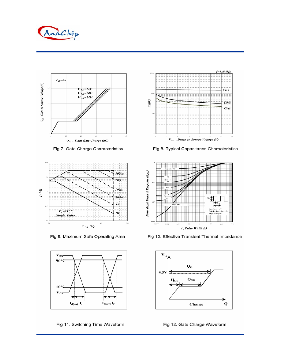
Typical Performance Characteristics (Continued)
AF4920N
N-Channel Enhancement Mode Power MOSFET
Anachip Corp.
www.anachip.com.tw Rev. 1.0 Oct 13, 2005
5/5
Marking Information
SO-8
( Top View )
1
8
4 9 2 0 N
AA Y W X
Year code:
Part Number
Lot code:
Week code:
Factory code
"A~Z": 01~26;
"A~Z": 27~52
"4" =2004
~
"A~Z": 01~26;
"A~Z": 27~52
"X": Non-Lead Free; "X": Lead Free
Logo
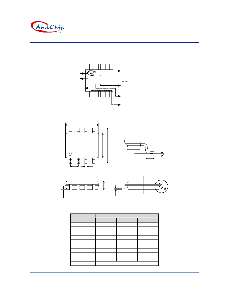
Package Information
Package Type: SO-8
L
E
E1
D
8
7
6
5
1
2
3
4
e
B
DETAIL A
1. All Dimensions Are in Millimeters.
2. Dimension Does Not Include Mold Protrusions.
C
DETAIL A
A
A1
Dimensions In Millimeters
Symbol
Min.
Nom.
Max.
A
1.35 1.55 1.75
A1 0.10 0.18 0.25
B
0.33 0.41 0.51
C
0.19 0.22 0.25
D
4.80 4.90 5.00
E
5.80 6.15 6.50
E1 3.80 3.90 4.00
L
0.38 0.71 1.27
0
o
4
o
8
o
e 1.27
TYP.