AF8510C
N AND P-CHANNEL ENHANCEMENT MODE POWER MOSFET
This datasheet contains new product information. Anachip Corp. reserves the rights to modify the product specification without notice. No liability is assumed as a result of the use of
this product. No rights under any patent accompany the sale of the product.
Rev. 1.0 Nov 14, 2005
1/8
Features
- Lower On-Resistance
- Simple Drive Requirement
- Fast Switching Performance
- Pb Free Plating Product
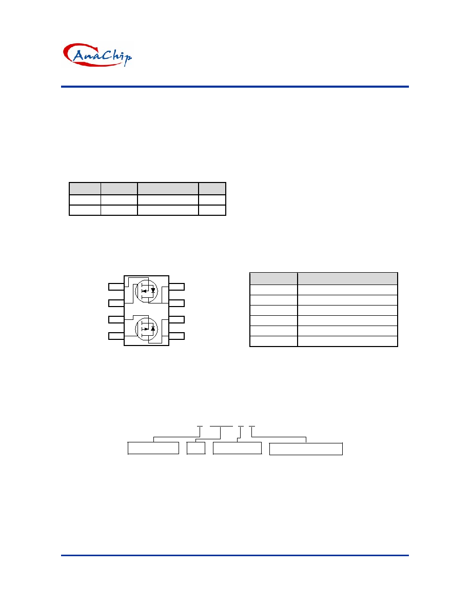
Product Summary
CH
BV
DSS
(V)
R
DS(ON)
(m)
I
D
(A)
N 30
28 6.9
P -30
55
-5.3
Pin Assignments
SO-8
5
6
7
8
4
3
2
1
D1
D1
D2
D2
S1
G1
S2
G2
General Description
The advanced power MOSFET provides the designer
with the best combination of fast switching,
ruggedized device design, low on-resistance and
costeffectiveness.
The SO-8 package is universally preferred for all
commercial-industrial surface mount applications and
suited for low voltage applicat ions such as DC/DC
converters.
Pin Descriptions
Pin Name
Description
S1 Source
(NMOS)
G1 Gate
(NMOS)
D1 Drain
(NMOS)
S2 Source
(PMOS)
G2 Gate
(PMOS)
D2 Drain
(PMOS)
Ordering information
A X 8510C X X
PN
Package
Feature
F :MOSFET
S: SOP-8
Packing
Blank : Tube or Bulk
A : Tape & Reel
AF8510C
N AND P-CHANNEL ENHANCEMENT MODE POWER MOSFET
Anachip Corp.
www.anachip.com.tw Rev. 1.0 Nov 14, 2005
2/8
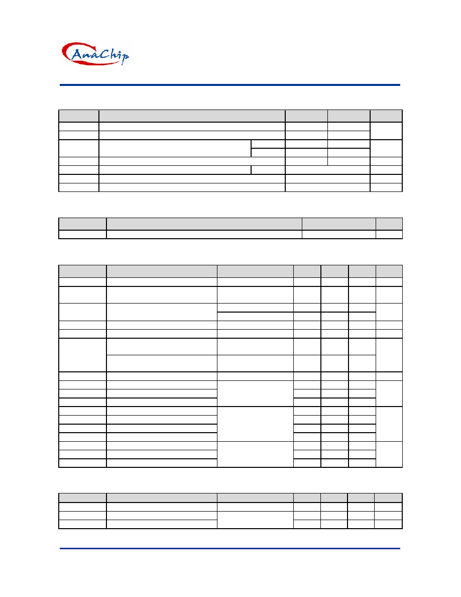
Absolute Maximum Ratings
Symbol
Parameter
N-Channel P-Channel
Units
V
DS
Drain-Source
Voltage
30
-30
V
GS
Gate-Source
Voltage
�20
�20
V
T
A
=25�C
6.9 -5.3
I
D
Continuous
Drain
Current
(Note 1)
T
A
=70�C
5.5 -4.2
V
I
DM
Pulsed Drain Current
(Note 2)
30
-30
A
P
D
Total
Power
Dissipation
T
A
=25�C
2.0 W
Linear Deratomg Factor
0.016
W/ �C
T
J
, T
STG
Operating Junction and Storage Temperature Range
-55 to 150
�C
Thermal Data
Symbol
Parameter
Maximum
Units
Rthj-amb Thermal
Resistance
Junction-ambient
(Note 1)
Max.
62.5 �C/W
N-CH Electrical Characteristics
at T
J
=25�C unless otherwise specified
Symbol
Parameter
Test Conditions
Min.
Typ.
Max.
Units
BV
DSS
Drain-Source
Breakdown
Voltage V
GS
=0V, I
D
=250uA 30
- - V
BV
DSS
/ T
J
Breakdown Voltage Temperature
Coefficient
Reference to 25
o
C,
I
D
=1mA
- 0.02 - V/
o
C
V
GS
=10V, I
D
=5A -
-
28
R
DS(ON)
Static Drain-Source
On-Resistance
(Note 3)
V
GS
=4.5V, I
D
=3A -
-
40
m
V
GS(th)
Gate Threshold Voltage
V
DS
=V
GS
, I
D
=250uA 1 - 3 V
g
fs
Forward
Transconductance V
DS
=10V, I
D
=5A
- 4.6 - S
Drain-Source Leakage Current
(T
J
=25
o
C)
V
DS
=30V, V
GS
=0V -
-
1
I
DSS
Drain-Source Leakage Current
(T
J
=70
o
C)
V
DS
=24V, V
GS
=0V -
-
25
uA
I
GSS
Gate-Source
Leakage
V
GS
=�20V -
-
�100
nA
Q
g
Total
Gate
Charge
(Note 3)
-
10
16
Q
gs
Gate-Source
Charge
- 2 -
Q
gd
Gate-Drain
("Miller")
Charge
I
D
=6.9A,
V
DS
=24V,
V
GS
=4.5V
- 6 -
nC
t
d(on)
Turn-On Delay Time
(Note 3)
-
8
-
t
r
Rise
Time
- 7 -
t
d(off)
Turn-Off Delay Time
-
20
-
t
f
Fall-Time
V
DS
=15V,
I
D
=1A,
R
G
=3.3, V
GS
=10V
R
D
=15
- 6 -
ns
C
iss
Input
Capacitance
- 540
870
C
oss
Output
Capacitance
- 160 -
C
rss
Reverse
Transfer
Capacitance
V
GS
=0V,
V
DS
=25V,
f=1.0MHz
- 120 -
pF
Source-Drain Diode
Symbol
Parameter
Test Conditions
Min.
Typ.
Max.
Unit
V
SD
Forward On Voltage
(Note 3)
I
S
=1.7A, V
GS
=0V -
-
1.2
V
t
rr
Reverse
Recovery
Time
- 20 - ns
Q
rr
Reverse Recovery Charge
I
S
=6.9A, V
GS
=0V
dl/dt=100A/�s
- 11 - nC
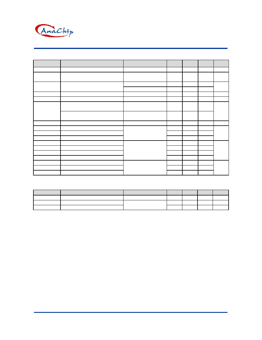
AF8510C
N AND P-CHANNEL ENHANCEMENT MODE POWER MOSFET
Anachip Corp.
www.anachip.com.tw Rev. 1.0 Nov 14, 2005
3/8
P-CH Electrical Characteristics
at T
J
=25�C unless otherwise specified
Symbol
Parameter
Test Conditions
Min.
Typ.
Max.
Units
BV
DSS
Drain-Source
Breakdown
Voltage V
GS
=0V, I
D
=250uA -30
- - V
BV
DSS
/
T
J
Breakdown Voltage Temperature
Coefficient
Reference to 25
o
C,
I
D
=1mA
- -0.023 - V/
o
C
V
GS
=-10V, I
D
=-5A -
-
55
V
GS
=-4.5V, I
D
=-3A -
-
90
m
V
GS(th)
Gate Threshold Voltage
V
DS
=V
GS
, I
D
=-250uA 1 - -3 V
g
fs
Forward
Transconductance V
DS
=-10V, I
D
=-5A
- 4.9 - S
Drain-Source Leakage Current
(T
J
=25
o
C)
V
DS
=-30V, V
GS
=0V - -
-1
I
DSS
Drain-Source Leakage Current
(T
J
=70
o
C)
V
DS
=-24V, V
GS
=0V - -
-25
uA
I
GSS
Gate-Source
Leakage
V
GS
=�20V -
-
�100
nA
Q
g
Total Gate Charge (Note 3)
- 9 15
Q
gs
Gate-Source
Charge
- 2 -
Q
gd
Gate-Drain
("Miller")
Charge
I
D
=-5.3A,
V
DS
=-24V,
V
GS
=-4.5V
- 6 -
nC
t
d(on)
Turn-On Delay Time (Note 3)
- 10 -
t
r
Rise
Time
- 8 -
t
d(off)
Turn-Off Delay Time
-
25
-
t
f
Fall-Time
V
DS
=-15V,
I
D
=1A,
R
G
=3.3, V
GS
=-10V
R
D
=15
- 13 -
ns
C
iss
Input
Capacitance
- 580
930
C
oss
Output
Capacitance
- 180 -
C
rss
Reverse
Transfer
Capacitance
V
GS
=0V,
V
DS
=25V,
f=1.0MHz
- 120 -
pF
Source-Drain Diode
Symbol
Parameter
Test Conditions
Min.
Typ.
Max.
Unit
V
SD
Forward On Voltage
(Note 3)
I
S
=1.7A, V
GS
=0V -
-
-1.2
V
t
rr
Reverse
Recovery
Time
)
- 21 - ns
Q
rr
Reverse Recovery Charge
I
S
=-5.3A, V
GS
=0V,
dl/dt=100A/�s
- 17 - nC
Note 1: Surface mounted on 1 in
2
copper pad of FR4 board; 135
o
C/W when mounted on Min. copper pad.
Note 2: Pulse width limited by Max. junction temperature.
Note 3: Pulse width 300us, duty cycle 2%.
AF8510C
N AND P-CHANNEL ENHANCEMENT MODE POWER MOSFET
Anachip Corp.
www.anachip.com.tw Rev. 1.0 Nov 14, 2005
4/8
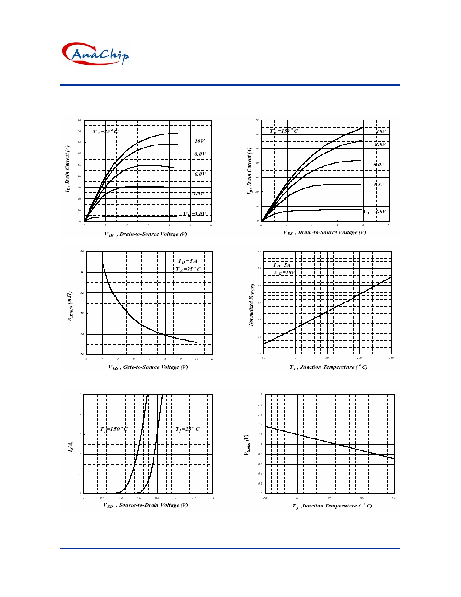
Typical Performance Characteristics (N-Channel)
Fig 1. Typical Output Characteristics
Fig 2. Typical Output Characteristics
Fig 3. On-Resistance v.s. Gate Voltage
Fig 4. Normalized On-Resistance v.s. Junction
Temperature
Fig 5. Forward Characteristic of Reverse Diode
Fig 6. Gate Threshold Voltage v.s. Junction
Temperature
AF8510C
N AND P-CHANNEL ENHANCEMENT MODE POWER MOSFET
Anachip Corp.
www.anachip.com.tw Rev. 1.0 Nov 14, 2005
5/8
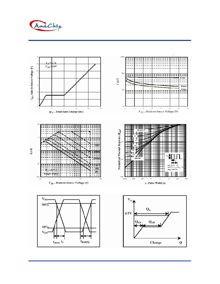
Typical Performance Characteristics (N-Channel) (Continued)
Fig 7. Gate Charge Characteristics
Fig 8. Typical Capacitance Characteristics
Fig 9. Maximum Safe Operation Area
Fig 10. Effective Transient Thermal Impedance
Fig 11. Switching Time Waveform
Fig 12. Gate Charge Waveform