 | –≠–ª–µ–∫—Ç—Ä–æ–Ω–Ω—ã–π –∫–æ–º–ø–æ–Ω–µ–Ω—Ç: AF9435PS | –°–∫–∞—á–∞—Ç—å:  PDF PDF  ZIP ZIP |

AF9435P
P-Channel 30-V (D-S) MOSFET
This datasheet contains new product information. Anachip Corp. reserves the rights to modify the product specification without notice. No liability is assumed as a result of the use of
this product. No rights under any patent accompany the sale of the product.
Rev. 1.1 Jul 20, 2004
1/5
Features
-Low r
DS(on)
Provides Higher Efficiency and Extends
Battery Life
-Miniature SO-8 Surface Mount Package Saves
Board Space
-High power and current handling capability
-Extended V
GS
range (±25) for battery pack
applications
Product Summary
V
DS
(V)
r
DS(on)
(m)
I
D
(A)
49@V
GS
=-10V
-5.7
-30
69@V
GS
=-4.5V
-5.0
Pin Assignments
SOP-8
5
6
7
8
4
3
2
1
D
D
D
D
S
S
S
G
General Description
These miniature surface mount MOSFETs utilize High
Cell Density process. Low r
DS(on)
assures minimal
power loss and conserves energy, making this device
ideal for use in power management circuitry. Typical
applications are PWMDC-DC converters, power
management in portable and battery-powered
products such as computers, printers, battery charger,
telecommunication power system, and telephones
power system.
Pin Descriptions
Pin Name
Description
S Source
G Gate
D Drain
Ordering information
A X 9435P X X X
PN
Package
Feature
F :MOSFET
S: SOP-8
Lead Free
Blank : Normal
L : Lead Free Package
Packing
Blank : Tube or Bulk
A : Tape & Reel
AF9435P
P-Channel 30-V (D-S) MOSFET
Anachip Corp.
www.anachip.com.tw Rev. 1.1 Jul 20, 2004
2/5
Absolute Maximum Ratings
(T
A
=25∫C unless otherwise noted)
Symbol
Parameter
Rating
Units
V
DS
Drain-Source
Voltage
-30
V
V
GS
Gate-Source
Voltage
±25
V
T
A
=25∫C ±6.5
I
D
Continuous
Drain
Current
(Note 1)
T
A
=70∫C ±5.2
A
I
DM
Pulsed Drain Current
(Note 2)
±30
A
I
S
Continuous Source Current (Diode Conduction)
(Note 1)
-1.6
A
T
A
=25∫C 3.1
P
D
Power
Dissipation
(Note 1)
T
A
=70∫C 2.0
W
T
J
, T
STG
Operating Junction and Storage Temperature Range
-55 to 150
∫C
Thermal Resistance Ratings
Symbol
Parameter
Maximum
Units
R
JC
Maximum
Junction-to-Case
(Note 1)
t
<
5 sec
25
∫C/W
R
JA
Maximum
Junction-to-Ambient
(Note 1)
t
<
5 sec
40
∫C/W
Note 1: surface Mounted on 1"x 1" FR4 Board.
Note 2: Pulse width limited by maximum junction temperature
Specifications
(T
A
=25∫C unless otherwise noted)
Limits
Symbol
Parameter
Test Conditions
Min.
Typ.
Max.
Unit
Static
V
(BR)DSS
Drain-Source breakdown Voltage
V
GS
=0V, I
D
=-250uA -30
- - V
V
GS(th)
Gate-Threshold
Voltage
V
DS
= V
GS
, I
D
=-250uA -1
-1.6
-3 V
I
GSS
Gate-Body
Leakage
V
DS
=0V, V
GS
=±25V -
-
±100
nA
V
DS
=-24V, V
GS
=0V -
-
-1
I
DSS
Zero Gate Voltage Drain Current
V
DS
=-24V, V
GS
=0V,
T
J
=55∫C
- - -5
uA
I
D(on)
On-State
Drain
Current
(Note 3)
V
DS
=-5V, V
GS
=-10V -30 - - A
V
GS
=-10V, I
D
=-5.7A -
38
49
V
GS
=-4.5V, I
D
=-5.0A -
54
69
r
DS(on)
Drain-Source
On-Resistance
(Note 3)
V
GS
=-10V, I
D
=-5.7A,
T
J
=55∫C
- 42 54
m
g
fs
Forward
Tranconductance
(Note 3)
V
DS
=-15V, I
D
=-5.7A -
19
-
S
V
SD
Diode Forward Voltage
I
S
=-2.1A, V
GS
=0V -
-0.7
-1.2
V
Dynamic
(Note 4)
Q
g
Total Gate Charge
-
6
11
Q
gs
Gate-Source
Charge
- 2.0 -
Q
gd
Gate-Drain
Charge
V
DS
=-15V, V
GS
=-4.5V,
I
D
=-5.7A
- 2.7 -
nC
Switching
t
d(on)
Turn-On Delay Time
-
7
14
t
r
Rise
Time
- 13 24
t
d(off)
Turn-Off Delay Time
-
14
25
t
f
Fall-Time
V
DD
=-15, R
L
=15,
I
D
=-1A, V
GEN
=-10V,
R
G
=6
- 9 17
nS
Note 3: Pulse test: PW < 300us duty cycle < 2%.
Note 4: Guaranteed by design, not subject to production testing.
AF9435P
P-Channel 30-V (D-S) MOSFET
Anachip Corp.
www.anachip.com.tw Rev. 1.1 Jul 20, 2004
3/5
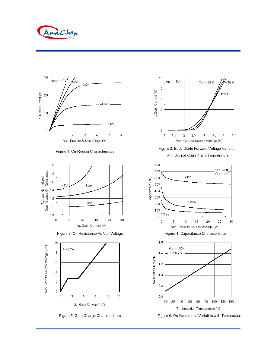
Typical Performance Characteristics

AF9435P
P-Channel 30-V (D-S) MOSFET
Anachip Corp.
www.anachip.com.tw Rev. 1.1 Jul 20, 2004
4/5
Typical Performance Characteristics
AF9435P
P-Channel 30-V (D-S) MOSFET
Anachip Corp.
www.anachip.com.tw Rev. 1.1 Jul 20, 2004
5/5
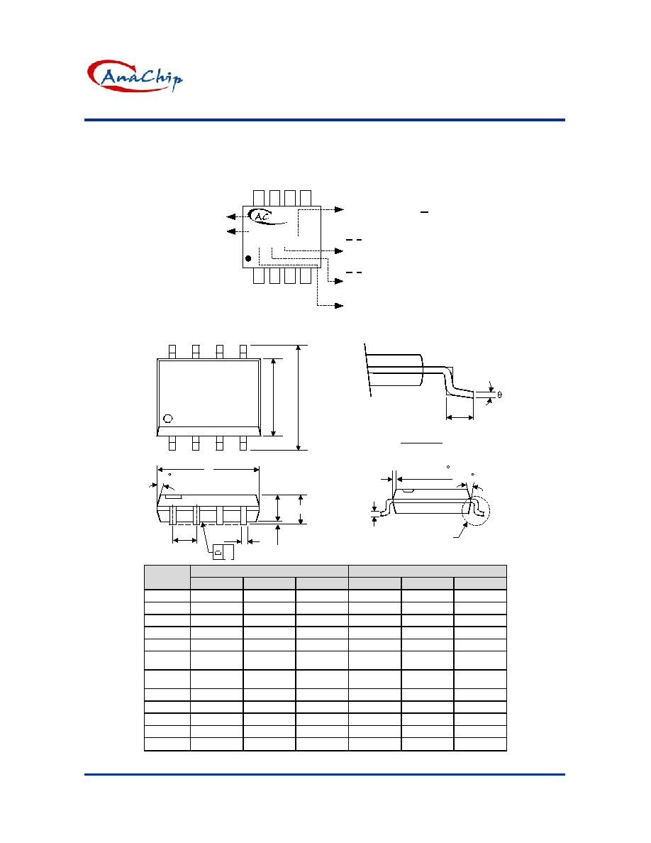
Marking Information
SOP-8L
( Top View )
1
8
9 4 3 5 P
AA Y W X
Year code:
Part Number
Lot code:
Week code:
Factory code
"A~Z": 01~26;
"A~Z": 27~52
"4" =2004
~
"A~Z": 01~26;
"A~Z": 27~52
"X": Non-Lead Free; "X": Lead Free
Logo
Package Information
Package Type: SOP-8L
VIEW "A"
L
C
VIEW "A"
H
E
A
A2
A1
B
e
D
7 (4X)
0.015x45
7 (4X)
y
Dimensions In Millimeters
Dimensions In Inches
Symbol
Min.
Nom.
Max.
Min.
Nom.
Max.
A 1.40 1.60 1.75 0.055 0.063 0.069
A1
0.10 - 0.25
0.040 - 0.100
A2 1.30 1.45 1.50 0.051 0.057 0.059
B 0.33 0.41 0.51 0.013 0.016 0.020
C 0.19 0.20 0.25 0.0075
0.008
0.010
D 4.80 5.05 5.30 0.189 0.199 0.209
E 3.70 3.90 4.10 0.146 0.154 0.161
e - 1.27 - - 0.050 -
H 5.79 5.99 6.20 0.228 0.236 0.244
L 0.38 0.71 1.27 0.015 0.028 0.050
y - - 0.10 - - 0.004
0
O
- 8
O
0
O
- 8
O