
AH276
Complementary Output Hall Effect Latch
This datasheet contains new product information. Anachip Corp. reserves the rights to modify the product specification without notice. No liability is assumed as a result of the use of
this product. No rights under any patent accompany the sale of the product.
Rev.1.0 Jul 21, 2005
1/6
Features
- On-chip Hall sensor with two different sensitivity
and hysteresis settings for AH276
- 400mA (avg) output sink current
- Built-in protecting diode only for chip reverse
power connecting
- -20
∞C to 85∞C operating temperature
- Low profile 4 pin SIP package
Applications
- Dual-coil Brush-less DC Motor
- Dual-coil Brush-less DC Fan
- Revolution Counting
- Speed Measurement
General Description
AH276 are integrated Hall sensors with output
drivers, mainly designed for electronic commutation
of brush-less DC Fan. This IC internally includes
the regulator, protecting diode, Hall plate, amplifier,
comparator, and a pair of complementary
open-collector outputs (DO, DOB).
While the magnetic flux density (B) is larger than
operate point (Bop), DO will turn on (low), and
meanwhile DOB will turn off (high). Each output is
latched until B is lower than release point (Brp),
and then DODOB transfer each state.
For DC fan application, sometimes need to test
power reverse connection condition. Internal diode
only protects chip-side but not for coil-side. If
necessary, add one external diode to block the
reverse current from coil-side.
Ordering Information
AH276 X - X X X
Packing
Blank : Tube or Bulk
P: SIP-4L
Package
Lead
L : Lead Free
Wafer Body
K: K version Wafer Body
Q: Q version Wafer Body
Typical Application Circuit
1 2
4
3
276
coil1
coil2
Vcc
Brush-less DC Fan
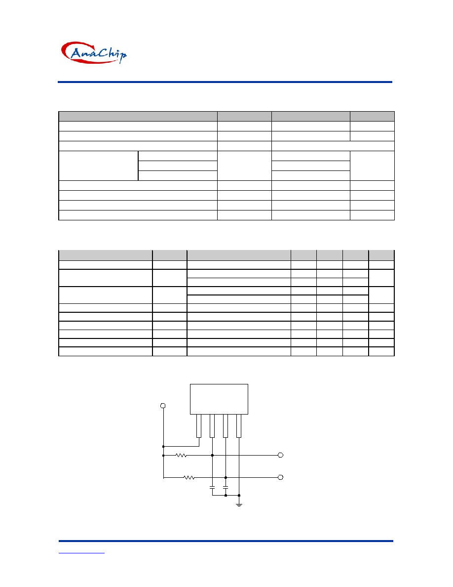
AH276
Complementary Output Hall Effect Latch
Anachip Corp.
www.anachip.com.tw
Rev.1.0 Jul 21, 2005
3/6
Absolute Maximum Ratings
( at Ta=25
∞C )
Characteristics
Symbol
Values
Unit
Supply voltage
V
CC
20 V
Reverse V
CC
Polarity Voltage
V
RCC
-20 V
Magnetic flux density
B
Unlimited
Continuous 0.4
Hold 0.5
Output "on" current
Peak (Start Up)
Ic
0.7
A
Operating temperature range
Ta
-20~+85
∞C
Storage temperature range
Ts
-65~+150
∞C
Package Power Dissipation
PD
550
mW
Maximum Junction Temp
Tj
150
∞C
Electrical Characteristics
(T=+25
∞C)
Characteristic
Symbol
Conditions
Min
Typ
Max
Units
Low Supply Voltage
Vce
Vcc=3.5V, I
L
=100mA -
0.4
-
V
K version
3.5
-
20
Supply Voltage
Vcc
Q version
2.5*
-
20
V
K version
-
46
-
Output Zener Breakdown
Vz
Q version
-
35
-
V
Output Saturation Voltage
Vce(sat) Vcc=14V, I
L
=400mA -
0.7
0.9
V
Output Leakage Current
Icex
Vce=14V, Vcc=14V
-
<0.1
10
µA
Supply Current
Icc
Vcc=20V, Output Open
-
16
25
mA
Output Rise Time
tr
Vcc=14V, R
L
=820, C
L
=20pF - 3.0
10 µs
Output Falling Time
tf
Vcc=14V, R
L
=820, C
L
=20pF - 0.3 1.5 µs
Switch Time Differential
t
Vcc=14V, R
L
=820, C
L
=20pF - 3.0
10 µs
*The output of DO/DOB will be switched on/off after supply voltage reaching the 2.5V.
Test Circuit
276
CL1 CL2
14V
DO
DOB
RL1=RL2=820 Ohm
CL1=CL2=20 pF
RL2
RL1
AH276
Complementary Output Hall Effect Latch
Anachip Corp.
www.anachip.com.tw
Rev.1.0 Jul 21, 2005
4/6
Magnetic Characteristics
(Ta=+25
∞C, V
CC
=12V)
K version (1mT = 10 Gauss)
Characteristic
Symbol
Min.
Typ.
Max.
Unit
Operate Point
Bop
-
-
110
Gauss
Release Point
Brp
-110
-
-
Gauss
Hysteresis Bhy
-
110
-
Gauss
Q version
Characteristic
Symbol
Min.
Typ.
Max.
Unit
Operate Point
Bop
5
-
70
Gauss
Release Point
Brp
-70
-
-5
Gauss
Hysteresis Bhy
-
-
Gauss
B
hy
V
sat
V
cc
(
Out
put
Vol
t
age )
B
rp
B
op
0
S
N
( Magnetic flux density B )
DO
Turn on
Turn off
( off-state )
( on-state )
B
hy
V
sat
V
cc
(
Out
put
Vol
t
age )
B
rp
B
op
0
S
N
( Magnetic flux density B )
DOB
Turn oFF
Turn on
( off-state )
( on-state )
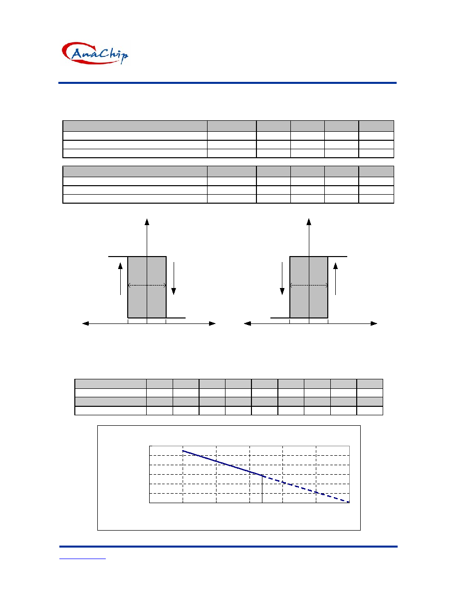
Performance Characteristics (SIP-4)
Ta (
∞C)
25
50
60
70
80
85
90
95
100
Pd
(mW)
550 440 396 352 308 286 264 242 220
Ta (
∞C)
105
110
115
120
125
130
135
140
150
Pd
(mW)
198 176 154 132 110 88 66 44 0
P o w e r D issip a tio n C u rve
0
1 0 0
2 0 0
3 0 0
4 0 0
5 0 0
6 0 0
0
2 5
5 0
7 5
1 0 0
1 2 5
1 5 0
T a ( C )
P d (m W )
8 5
AH276
Complementary Output Hall Effect Latch
Anachip Corp.
www.anachip.com.tw
Rev.1.0 Jul 21, 2005
5/6
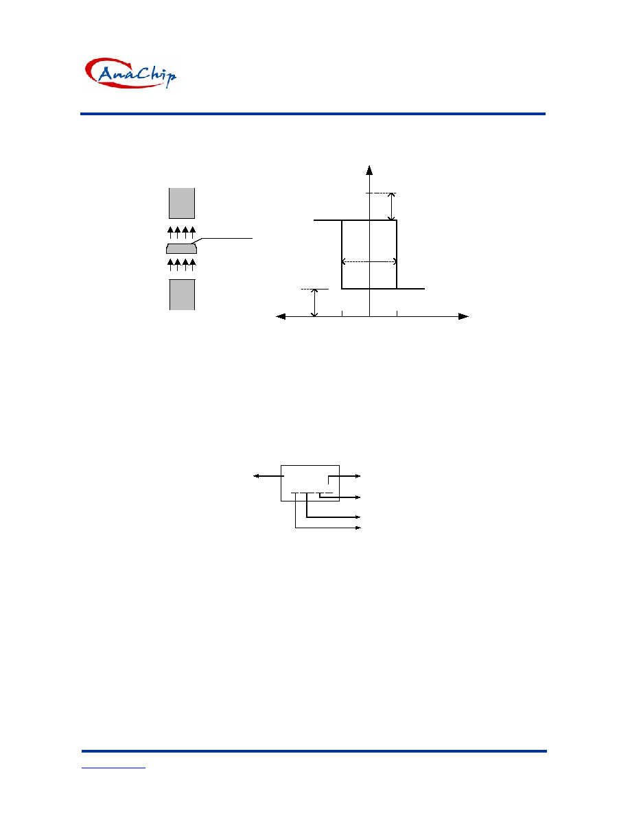
Operating Characteristics
Marking side
S
B
hy
V
sat
V
cc
( Output Voltage )
V
d
B
rp
B
op
0
S
N
( Magnetic flux density )
DO
High
Low
( SIP4 )
N
Marking Information
276
Part Number
Year:
( Top View )
"2" = 2002
"1" = 2001
X XX X X
Nth week: 01~52
K: AH276K-PL
Wafer Lot ID: a~z
~
Q: AH276Q-PL

