
AH337
Single Phase Hall Effect Switch
This datasheet contains new product information. Anachip Corp. reserves the rights to modify the product specification without notice. No liability is assumed as a result of the use of
this product. No rights under any patent accompany the sale of the product.
Rev.1.2 Mar. 29, 2006
1/8
Features
- 4.2V to 28V DC operation voltage
- Temperature compensation
- Wide operating voltage range
- Open drain pre-driver
- 25mA maximum sinking output current.
- Package: SIP3, SOT23
Applications
- VCD/DVD loader, CD/DVD ROM
- Cover detector
- Speed measurement
- Home appliances
- Home safety
General Description
AH337 is an switched Hall-Effect IC which is for
contactless switching applications. The device
includes an on-chip Hall voltage generator for
magnetic sensing, an amplifier that amplifies the
Hall voltage, a schmitt trigger to provide switching
hysteresis for noise rejection, and an open-drain
output. The bandgap regulator allows a wide
operating voltage range.
If a magnetic flux density larger than threshold Bop,
DO is turned on(low). The output state is held until
a magnetic flux density reversal falls below Brp
causing DO to be turned off (high).
Pin Assignment
337
1
2 : GND
3 : OUT
2
3
337
1
2
3
1 : Vdd
(Top view)
(SIP package)
(SOT23 package)
Pin Descriptions
Name
P/I/O
Pin #
Description
Vdd
P 1
Positive Power Supply
GND
P 2
Ground
OUT
O 3
Output Pin
Ordering Information
AH337 X - X X X
Packing
P: SIP3
W: SOT23
Package
Lead
L : Lead Free
Wafer Body
Blank or
A~Z : if necessary
to specify
Spread-leg ammo pack for SIP-3L;
Blank : Bulk
A :
Tape & Reel for SOT23

AH337
Single Phase Hall Effect Switch
Anachip Corp.
www.anachip.com.tw
Rev.1.2 Mar. 29, 2006
2/8
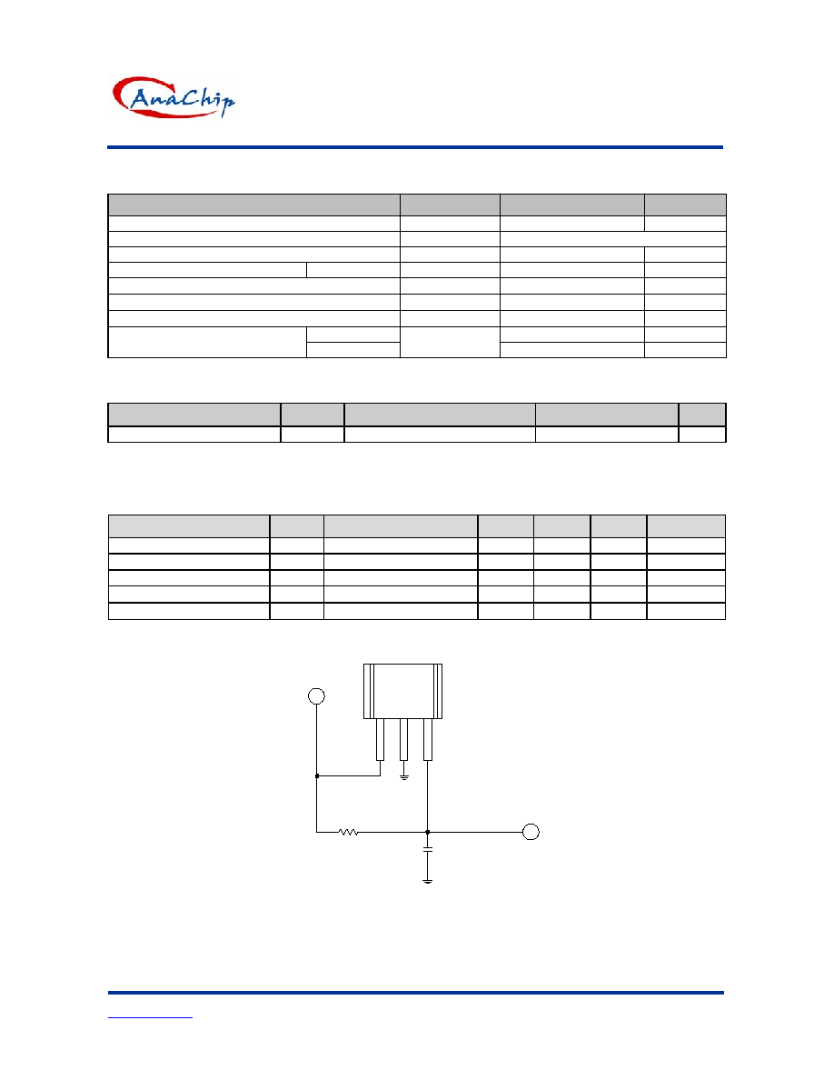
Typical Application Circuit
AH337
4.2V ~28V
Digital Output
Vdd
OUT
GND
L
R
Functional Block Diagrams
Regulator
Hall
plate
Amp
2
GND
OUT
3
2
Vdd
1
AH337
Single Phase Hall Effect Switch
Anachip Corp.
www.anachip.com.tw
Rev.1.2 Mar. 29, 2006
3/8
Absolute Maximum Ratings
( at Ta=25
o
C )
Characteristics
Symbol
Values
Unit
Supply Voltage
Vdd
30
V
Magnetic Flux Density
B
Unlimited
Output OFF Voltage
V
DS
30 V
Output "ON" Current
Continuous
Id
25
mA
Operating Temperature Range
Ta
-40~+125
�C
Storage Temperature Range
Ts
-65~+150
�C
Maximum Junction Temp.
Tj
150
�C
SIP-3L 550
mW
Package Power Dissipation
SOT23-3L
Pd
230 mW
Recommended Operating Conditions
( Ta=25
o
C )
Paramter
Symbol
Conditions
Rating
Unit
Supply Voltage
Vdd
Operating
4.2*~28
V
*Note: The output of IC will be switched after the supply voltage is over 4.2V, but the magnetic characteristics won't be normal until the
supply is over 4.5V.
Electrical Characteristics
(Ta=+ 25
�C, Vdd=12V)
Characteristic
Symbol
Test Conditions
Min
Typ
Max
Units
Output Saturation Voltage V
DS(sat)
Iout=10mA,
B
>
Bop
-
300
400
mV
Output Leakage Current
Ioff
B < Brp
-
<0.1
10 uA
Supply Current
Idd
Output Open
-
2
4
mA
Output Rise Time
tr
RL=820
, CL=20pF
- 0.1 1 us
Output Falling Time
tf
RL=820
, CL=20pF
- 0.1 1 us
Test Circuit
CL
12V
OUT
RL=820 Ohm
CL=20 pF
RL
Test Circuit
AH337
Single Phase Hall Effect Switch
Anachip Corp.
www.anachip.com.tw
Rev.1.2 Mar. 29, 2006
4/8
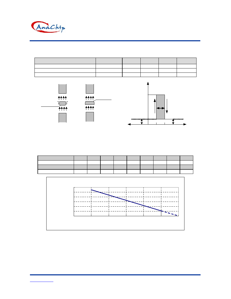
Magnetic Characteristics
(Ta=25
�C, Vdd=4.5V to 28V)
(1mT=10Gauss)
Parameter
Symbol
Min.
Typ.
Max.
Unit
Operate Point
Bop
90
120
150
Gauss
Release Point
Brp
30
60
90
Gauss
Hysteresis Bhys
-
60
-
Gauss
Marking side
S
( SIP3 )
N
Marking side
S
( SOT23 )
N
B
h
y
V
dd
(
O
u
t
put
Vol
t
age
)
B
rp
B
op
0
( Magnetic flux density B )
Output
Turn off
Turn on
( off-state )
( on-state )
V
sat
V
sat
Performance Characteristics (SIP3)
Ta (
�C)
25
50
60
70
80
85
90
95
100
Pd
(mW)
550 440 396 352 308 286 264 242 220
Ta (
�C)
105
110
115
120
125
130
135
140
150
Pd
(mW)
198 176 154 132 110 88 66 44 0
P o w e r D is s ip a tio n C u rv e
0
1 0 0
2 0 0
3 0 0
4 0 0
5 0 0
6 0 0
0
2 5
5 0
7 5
1 0 0
1 2 5
1 5 0
T a ( C )
P d (m W )
AH337
Single Phase Hall Effect Switch
Anachip Corp.
www.anachip.com.tw
Rev.1.2 Mar. 29, 2006
5/8
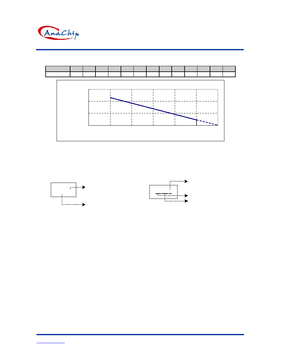
Performance Characteristics (SOT23-3)
Ta (
�C)
25
50
60
70
80
90
100
110
120
125
130 140 150
Pd
(mW) 230 184 166 147
129
110
92
74
55
46
37 18 0
P o w e r D is s ip a tio n C u rv e
0
1 0 0
2 0 0
3 0 0
0
2 5
5 0
7 5
1 0 0
1 2 5
1 5 0
T a ( C )
P d (m W )
Marking Information
(1) SIP3
(2) SOT23
337
YWW X
Date code
Y : Year
WW : Nth week
(Top View)
ID Code:
A~Z: Non-Lead Free
a~z : Lead Free
P1:AH337
XX YM X
Date code
Y : Year
M :Month(A~L)
(Top View)
ID code
A~Z: Non-Lead Free
a~z: Lead Free
AH337
Single Phase Hall Effect Switch
Anachip Corp.
www.anachip.com.tw
Rev.1.2 Mar. 29, 2006
6/8
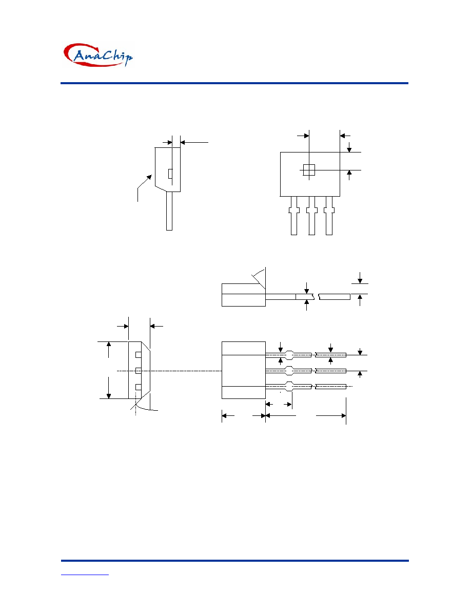
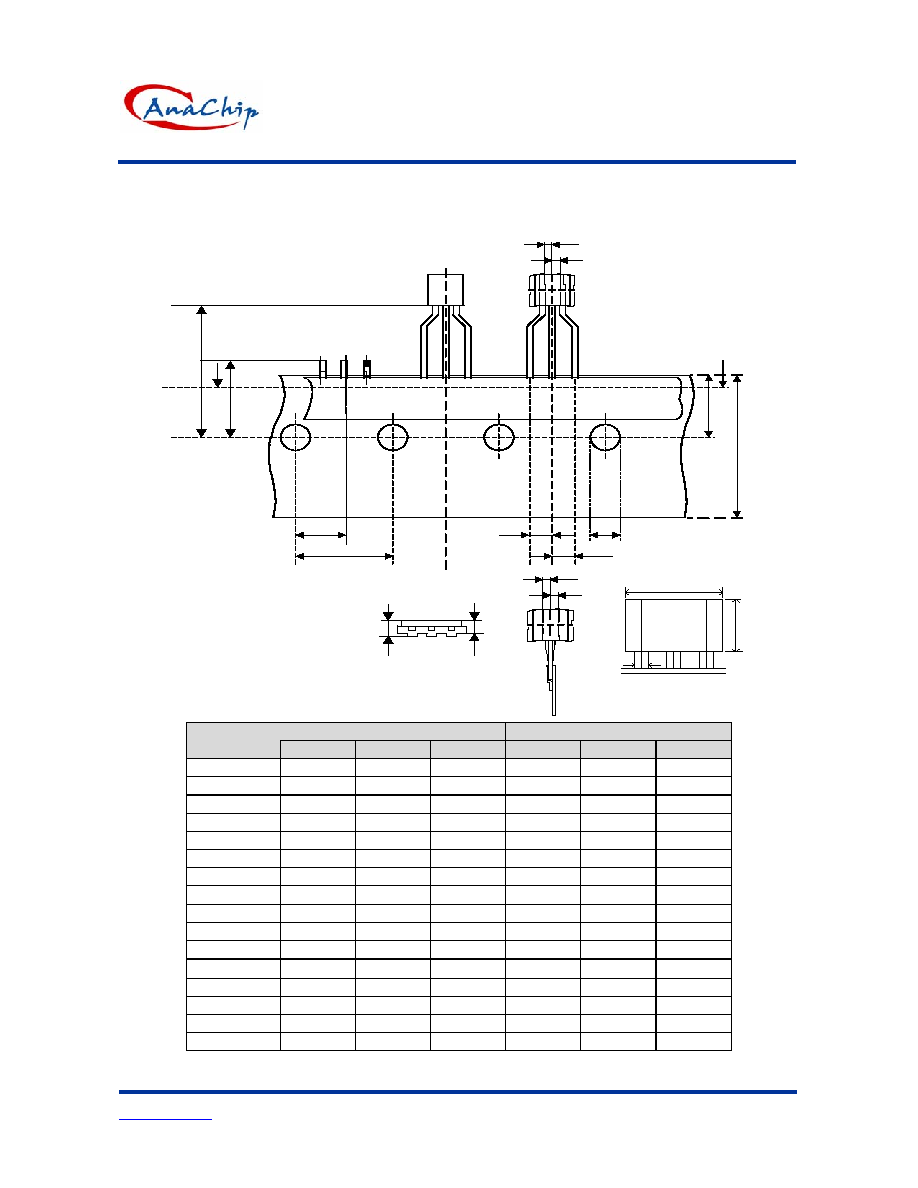
Package Information
(unit: mm)
(1) Package Type: SIP-3L for Bulk Pack
Active Area Depth
Sensor Location
1
2
3
2.00mm
1.15mm
0.51mm
NOM
BRANDED
SURFACE
Package Dimension
1.57mm
1.47mm
4.17mm
4.04mm
1.82
mm
15.50mm
13.00mm
1
2
3
1.27mm
0.41mm
0.41mm
45�
45�
0.38mm
0.7mm
3.10mm
2.97mm
AH337
Single Phase Hall Effect Switch
Anachip Corp.
www.anachip.com.tw
Rev.1.2 Mar. 29, 2006
7/8
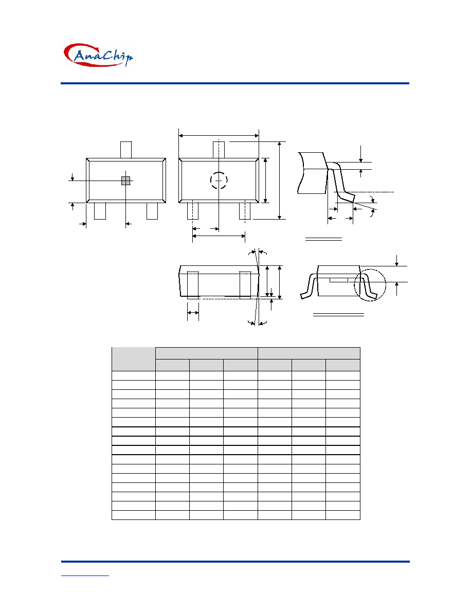
Package Information (Continued)
(2) Package Type: Spread leg SIP-3L for Ammo-Pack only
P o
W
F 2
F 1
W 1
H
D 0
B
A
L
P 2
p
p
h
h
A
D
b 2
T 1
T
A n s ic h t A -B
v ie w A -B
Dimensions In Millimeters
Dimensions In Inches
Symbol
Min.
Nom.
Max.
Min.
Nom.
Max.
A 2.80
3.00
3.20
0.110
0.118
0.125
D 3.90
4.10
4.30
0.153
0.161
0.169
b2
0.33
0.38
0.42
0.012
0.014
0.016
D0 3.80
4.00
4.20
0.149
0.157
0.165
F1 2.35
2.55
2.75
0.092
0.100
0.108
F2 2.45
2.55
2.85
0.096
0.100
0.112
H - -
20
- -
0.787
h
- - 1 - -
0.039
L -
-
11
-
-
0.433
P0 12.2 12.7 13.2 0.480 0.5 0.519
P2
5.95 6.35 6.75 0.234 0.25 0.265
p
- - 1 - -
0.039
T - -
0.55
- -
0.021
T1 - -
1.42
- -
0.055
W 17.5
18.0
18.5
0.688
0.708
0.728
W1 5.5
6.0
6.5
0.216
0.236
0.255
Package Information (Continued)
AH337
Single Phase Hall Effect Switch
Anachip Corp.
www.anachip.com.tw
Rev.1.2 Mar. 29, 2006
8/8
(3) Package Type: SOT23-3L
e
E
HE
D
A2
A1
b(3x)
A
2(4x)
e1
2
1
3
1.45mm
0.8mm
( Sensing point )
1(4x)
L
VIEW C
L1
GAUGE PLANE
C
SEE VIEW C
M
Dimensions In Millimeters
Dimensions In Inches
Symbol
Min.
Nom.
Max.
Min.
Nom.
Max.
A 1.05 - 1.35
0.041 - 0.053
A1 0.05 - 0.15
0.002 - 0.006
A2 1.00 1.10 1.20 0.039
0.043 0.047
b 0.25 - 0.50
0.010
-
0.020
C 0.08 - 0.20
0.003
-
0.008
D
2.70 2.90 3.00 0.106
0.114 0.118
E
1.50 1.60 1.70 0.059
0.063 0.067
HE 2.60 2.80 3.00 0.102
0.110 0.118
L 0.30 - 0.60
0.012
-
0.024
L1 0.50 0.60 0.70 0.020
0.024 0.028
M
0.73 0.78 0.83 0.029
0.031 0.033
e
1.80 1.90 2.00 0.071
0.075 0.079
e1 0.85 0.95 1.05 0.033
0.037 0.041
0
o
5
o
10
o
0
o
5
o
10
o
1 3
o
5
o
7
o
3
o
5
o
7
o
2 6
o
8
o
10
o
6
o
8
o
10
o