
AM93LC86
16384-bits Serial Electrically Erasable PROM
(Preliminary)
This datasheet contains new product information. Anachip Corp. reserves the rights to modify the product specification without notice. No liability is assumed as a result of the use of
this product. No rights under any patent accompany the sale of the product.
Rev 0.1 Oct 20, 2003
1/12
Features
∑ State-of-the-art architecture
- Non-volatile data storage
- Standard voltage and low voltage operation
Vcc: 2.7V ~ 5.5V
- Full TTL compatible inputs and outputs
- Auto increment read for efficient data dump
∑ Hardware and software write protection
- Software instructions for write-enable/disable
-
VCC level verification before self-timed
programming cycle
∑ Versatile, easy-to-use interface
- Self-timed programming cycle
- Automatic erase-before-write
- Programming status indicator
- Word and chip erasable
- Stop SK anytime for power savings
∑ Durability and reliability
- 40 years data retention
- Minimum of 1M write cycles per word
- Unlimited read cycles
- ESD protection
Pin Assignments
1
3
2
4
8
6
7
5
1
3
2
4
8
6
7
5
PDIP Package
SOP Package
1
3
2
4
8
6
7
5
TSSOP Package
CS
SK
DI
DO
CS
SK
DI
DO
VCC
ORG
GND
WP
VCC
ORG
GND
WP
VCC
ORG
GND
WP
CS
SK
DI
DO
General Description
The AM93LC86 is the 16384-bit non-volatile serial
EEPROM. The AM93LC86 provides efficient
non-volatile read/write memory arranged as 1024
words of 16 bits each when the ORG Pin is
connected to VCC and 2048 words of 8 bits each
when it is tied to ground. The instruction set
includes read, write, and write enable/disable
functions. The data out pin (DO) indicates the
status of the device during the self-timed
non-volatile programming cycle.
The self-timed write cycle includes an automatic
erase-before-write capability. Only when the chip is
in the write enable state and proper Vcc operation
range is the write instruction accepted and thus to
protect against inadvertent writes. Data is written in
16 bits per write instruction into the selected
register. If chip select (CS) is brought high after
initiation of the write cycle, the data output (DO) pin
will indicate the read/busy status of the chip.
The AM93LC86 is available in space-saving 8-lead
PDIP, SOP and TSSOP packages.
Pin Descriptions
(note)
Name
Description
CS Chip
select
SK Serial
clock
DI Data
input
DO Data
output
GND Ground
VCC Power
supply
WP
Write protection (active low)
ORG Organization
Note: See pin descriptions (continued) for more details
Ordering Information
Type
Package
86: 16K
S : SOP-8L
N : PDIP-8L
TS: TSSOP-8L
Temp. grade
AM93 LC 86 X X X
Packing
Blank : Tube
A : Taping
Operating Voltage
LC : 2.7V~5.5V,CMOS
Blank :
C
o
70
~
C
o
0
+
I :
C
o
85
~
C
o
40
+
-

AM93LC86
16384-bits Serial Electrically Erasable PROM
(Preliminary)
Anachip Corp.
www.anachip.com.tw
Rev 0.1 Oct 20, 2003
2/12
Block Diagram
Instruction
register
(13/14 bits)
Instruction
decode control
and
clock generation
Data register
Address register
V
CC
range
detector
Write enable
Dummy bit
R/W AMPS
Decoder
High voltage
generator
EEPROM
array
(1024 X 16)
or
(2048 X 8)
DI
CS
SK
DO
ORG
WP
VCC
GND
Absolute Maximum Ratings
Symbol
Parameter
Rating
Unit
T
STG
Storage temperature
-65 to +125
∞C
V
CC
Voltage with respect to ground
-0.3 to + 6.5
V
T
OP
Temperature under bias
0 to + 70
∞C
Note: These are stress rating only. Appropriate conditions for operating these devices given elsewhere may permanently damage the
part. Prolonged exposure to maximum ratings may affect device reliability.
AM93LC86
16384-bits Serial Electrically Erasable PROM
(Preliminary)
Anachip Corp.
www.anachip.com.tw
Rev 0.1 Oct 20, 2003
3/12
DC Electrical Characteristics
(Vcc =2.7~5.5V, T
A
= 25
o
C, unless otherwise noted)
Symbol
Parameter
Conditions
Min
Max
Unit
I
CC
Operating current**
CS=V
IH
, SK=1MHz CMOS input levels
3
mA
I
SB
Standby current
CS=DI=SK=0V
10
µA
I
IL
Input leakage
V
IN
= 0V to V
CC(CS,SK,DI)
-1
1
µA
I
OL
Output leakage
V
OUT
= 0V to V
CC
, CS=0V
-1
1
µA
V
CC
= 3V + 10%
-0.1
0.15 V
CC
V
IL
Input low voltage**
V
CC
= 5V + 10%
-0.1
0.8
V
V
CC
= 3V + 10%
0.8 V
CC
V
CC
+0.2
V
IH
Input high voltage**
V
CC
= 5V + 10%
2
V
CC
+0.2
V
V
OL1
Output low voltage
I
OL
= 2.1mA TTL, V
CC
=5V + 10%
0.4
V
V
OH1
Output high voltage
I
OH
= -400uA TTL, V
CC
=5V + 10%
2.4
V
V
OL2
Output low voltage
I
OL
= 10uA CMOS
0.2
V
V
OL2
Output high voltage
I
OH
= -10uA CMOS
V
CC
-0.2 V
Note ** : I
CC
, V
IL
min and V
IH
max are for reference only and are not tested.
AC Electrical Characteristics
(Vcc = 2.7V ~ 5.5V, T
A
= 25
o
C, unless otherwise noted)
Symbol
Parameter
Conditions
Min
Max
Unit
F
SK
SK
Clock
Frequency
0 1 Mhz
T
SKH
SK High Time
250
nS
T
SKL
SK Low Time
250
nS
T
CS
Minimum CS Low Time
250
nS
T
CSS
CS Setup Time
Relative to SK
50
nS
T
DIS
DI Setup Time
Relative to SK
100
nS
T
CSH
CS Hold Time
Relative to SK
0
nS
T
DIH
DI Hold Time
Relative to SK
100
nS
T
PD1
Output Delay to "1"
AC test (Fig. 1)
500
nS
T
PD0
Output Delay to "0"
AC test (Fig. 1)
500
nS
T
SV
CS to Status Valid
AC test CL = 100pF
500
nS
T
DF
CS to DO in 3-state
CS = VIL
100
nS
T
WP
Write
Cycle
Time
10 mS
Endurance
(note)
5V, 25∫C
1M
write cycles
Note: The parameter is characterized and isn't 100% tested.
632 ohm
DO
1.247V
(1 TTL Gate Load)
100PF
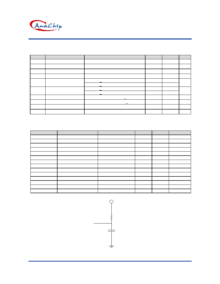
Figure 1. AC test circuit
AM93LC86
16384-bits Serial Electrically Erasable PROM
(Preliminary)
Anachip Corp.
www.anachip.com.tw
Rev 0.1 Oct 20, 2003
4/12
Pin Capacitance
(note)
(T
A
=25
∞C, F=1Mhz )
Symbol
Parameter
Max
Unit
C
OUT
Output
capacitance 5
pF
C
IN
Input
capacitance 5
pF
Note: The parameter is characterized and isn't 100% tested.
Instruction Set
Address
Input data
Instruction
(note)
Start bit
Op code
X8
X16
◊
8
◊
16
READ 1 10 A
10
~ A
0
A
9
~ A
0
- -
EWEN 1 00
11XXXXXXXXX
11XXXXXXXX
- -
WRITE 1 01 A
10
~ A
0
A
9
~ A
0
D
7
≠ D
0
D
15
- D
0
WRAL 1 00
01XXXXXXXXX
01XXXXXXXX
D
7
≠ D
0
D
15
- D
0
EWDS 1 00
00XXXXXXXXX
00XXXXXXXX
- -
ERASE 1 11 A
10
~ A
0
A
9
~ A
0
- -
ERAL 1 00
10XXXXXXXXX
10XXXXXXXX
- -
Note:
READ: Read
EWDS: Erase/write disable
EWEN: Erase/write enable
ERASE: Erase
WRITE: Write
ERAL: Erase all
WRAL: Write all
Functional Description
Endurance and data retention
The AM93LC86 is designed for applications
requiring up to 1M programming cycles (WRITE,
WRAL, EARSE and ERAL). It provides 40 years of
secure data retention.
Device operation
The AM93LC86 is controlled by seven 13-bit
instructions. Instructions are clocked in (serially) on
the DI pin. Each instruction begins with a logical "1"
(the start bit). This is followed by the opcode (2 bits),
the address field (10/11 bits), and data, if
appropriated,. The clock signal (SK) may be halted
at any time and the AM93LC86 will remain in its last
state. This allows full static flexibility and maximum
power conservation.
Auto increment read operations
Sequential read is possible, since the AM93LC86
has been designed to output a continuous stream
of memory content in response to a single
read
operation instruction. To utilize this function, the
system asserts a read instruction specifying a start
location address. Once the 8-bit or 16-bit of the
addressed word have been clocked out, the data in
consecutively higher address locations is output.
The address will wrap around continuously with CS
high until the chip select (CS) control pin is brought
low. This allows for single instruction data dumps to
be executed with a minimum of firmware overhead.
Read (READ)
The READ instruction is the only instruction that
outputs serial data on the DO pin. After the read
instruction and address have been decoded, data is
transferred from the selected memory register into
a 8-bit or 16-bit serial shift register. (Please note
that one logical "0" bit precedes the actual 8-bit or
16-bit output data string.) The output on DO
changes during the rising edge transitions of SK.
(shown in figure 3)

AM93LC86
16384-bits Serial Electrically Erasable PROM
(Preliminary)
Anachip Corp.
www.anachip.com.tw
Rev 0.1 Oct 20, 2003
5/12
Functional Description
Erase/write enable (EWEN)
Before any device programming (WRITE, WRAL,
ERASE, and ERAL) can be done, the EWEN
instruction must be executed first. When Vcc is
applied, this device powers up in the EWDS state.
The device then remains in a erase/write disable
(EWDS) state until a EWEN instruction is executed.
Thereafter the device remains enabled until a
EWDS instruction is executed or until Vcc is
removed. (shown in Figure 4)
Note: Neither the EWEN nor the EWDS instruction
has any effect on the READ instruction.
Erase/write disable (EWDS)
The erase/write disable (EWDS) instruction
disables all programming capabilities. This protects
the entire part against accidental modification of
data until a EWEN instruction is executed. (When
Vcc is applied, this part powers up in the EWDS
state.) To protect data, a EWDS instruction should
be executed upon completion of each programming
operation.
Note:
Neither the EWEN nor the EWDS instruction has any effect on
the READ instruction. (shown in figure 5)
Write (WRITE)
The WRITE instruction includes 8-bit or 16-bit of
data to be written into the specified register. After
the last data bit has been applied to DI, and before
the next rising edge of SK, CS must be brought low.
The falling edge of CS initiates the self-timed
programming cycle. After a minimum wait of 250ns
(5V operation) from the falling edge of CS (tcs), DO
will indicate the READY/BUSY status of the chip if
CS is brought HIGH. This means that logical "0"
implies the programming is still in progress while
logical "1" indicates the selected register has been
written, and the part is ready for another instruction.
(shown in figure 6)
Note:
The combination of CS HIGH, DI HIGH and the rising edge of
the SK clock, resets the READY/BUSY flag. Therefore, it is
important if you want to access the READY/BUSY flag, not to
reset it through this combination of control signals.
Before a WRITE instruction can be executed, the
device must be in the Write enable (WEN) state.
Write all (WRAL)
The Write All (WRAL) instruction programs all
registers with the data pattern specified in the
instruction. While the WRAL instruction is being
loaded, the address field becomes a sequence of
DON'T-CARE bits. (Shown in Figure 7)
As with the WRITE instruction, if CS is brought
HIGH after a minimum wait of 250ns (tcs), the DO
pin indicates the READY/BUSY status of the chip.
(shown in figure 7)
Erase (ERASE)
After the erase instruction is entered, CS must be
brought LOW. The falling edge of CS initiates the
self-timed internal programming cycle. Bringing CS
HIGH after minimum of tcs, will cause DO to
indicate the READ/BUSY status of the chip. To
explain this, a logical "0" indicates the programming
is still in progress while a logical "1" indicates the
erase cycle is complete and the part is ready for
another instruction. (shown in figure 8)
Erase all (ERAL)
Full chip erase is provided for ease of programming.
Erasing the entire chip involves setting all bits in the
entire memory array to a logical "1". (shown in
figure 9)