 | ÐлекÑÑоннÑй компоненÑ: AP1117D30 | СкаÑаÑÑ:  PDF PDF  ZIP ZIP |
Microsoft Word - R120-3-014-A2 AP1117_920418 .doc
AP1117
1A Low Dropout Positive Adjustable or Fixed-Mode Regulator
This datasheet contains new product information. Analog Technology reserves the rights to modify the product specification without notice. No liability is assumed as a result of the
use of this product. No rights under any patent accompany the sale of the product.
Rev. A4. Apr. 18, 2003
1/7
ATC
Analog Technology,
Features
·
1.4V maximum dropout at full load current
·
Fast transient response
·
Output current limiting
·
Built-in thermal shutdown
·
Packages: SOT223, TO252, TO220, SOT89
·
Good noise rejection
·
3-Terminal Adjustable or Fixed 1.5V, 1.8V,2.5V,
3.3V, 5.0V
Applications
·
PC peripheral
·
Communication
General Description
AP1117 is a low dropout positive adjustable or
fixed-mode regulator with minimum of 1A output
current capability. The product is specifically
designed to provide well-regulated supply for low
voltage IC applications such as high-speed bus
termination and low current 3.3V logic supply.
AP1117 is also well suited for other applications
such as VGA cards. AP1117 is guaranteed to have
<1.3V dropout at full load current making it ideal to
provide well regulated outputs of 1.25 to 5.0 with 6.3
to 12V input supply.
Ordering Information
AP 1117 X XX X
Low Dropout Regulator
Package
Vout
E : SOT223-3L
D : TO252-3L
T : TO220-3L
Y : SOT89-3L
Blank : ADJ
15 : 1.5V
18 : 1.8V
25 : 2.5V
33 : 3.3V
50 : 5.0V
Packing
Blank : Tube
A : Taping
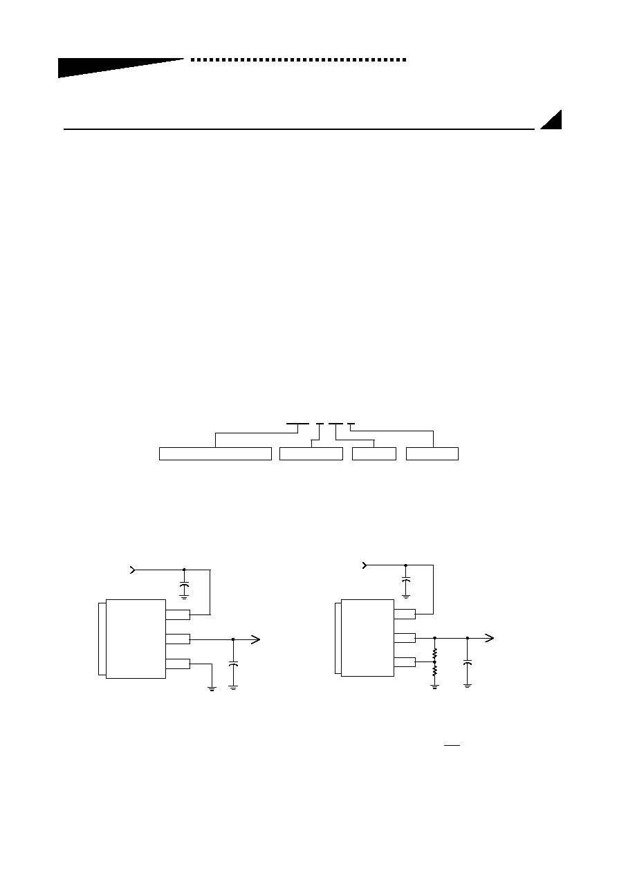
Typical Circuit
C2
100uF
5V
3.3V/1A
Tab is Vout
Vin
Vout
GND
C1
100uF
( 5V/3.3V fixed output )
R1
121
R2
121
C2
100uF
5V
2.5V/1A
Tab is Vout
Vin
Vout
Adj
C1
100uF
o
V
( 5V/2.5V ADJ output )
)
1
2
REF
o
R
R
(1
V
V
+
=
Note:
AP1117
1A Low Dropout Positive Adjustable or Fixed-Mode Regulator
Rev. A4 APR. 18, 2003
2/8
ATC
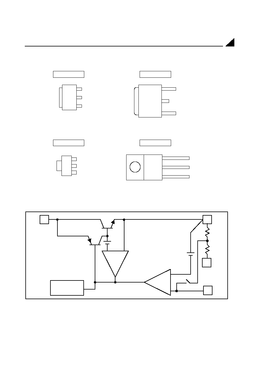
Connection Diagram
3 PIN SOT223
3 PIN TO252
3 PIN TO220
Vin
Vout
Adj (GND)
Tab is Vout
( Top View )
3
2
1
Vin
Vout
Adj (GND)
Tab is Vout
Tab is Vout
Vin
Vout
Adj (GND)
( Top View )
3 PIN SOT89
Adj (GND)
Vout
Vin
3
2
1
1
3
2
Tab is Vout
3
2
1
Block Diagram
3
Thermal
Shutdown
1
2 Vout
Adj
1.25V
+
+
CURRENT
LIMIT
Vin
-
+
-
+
1`
GND
(FIXED)
AP1117
1A Low Dropout Positive Adjustable or Fixed-Mode Regulator
Rev. A4 APR. 18, 2003
3/8
ATC
Pin Descriptions
NAME
I/O
PIN #
FUNCTION
Adj (GND)
I
1
A resistor divider from this pin to the Vout pin and ground sets the
output voltage. (Ground only for Fixed-Mode)
Vout
O
2
The output of the regulator. A minimum of 10uF capacitor must be
connected from this pin to ground to insure stability.
Vin
I
3
The input pin of regulator. Typically a large storage capacitor is
connected from this pin to ground to insure that the input voltage
does not sag below the minimum dropout voltage during the load
transient response. This pin must always be 1.3V higher than Vout
in order for the device to regulate properly.
Absolute Maximum Ratings
DC Supply Voltage (Vin)
........................................................ -0.3 to 12 V
Power Dissipation ......................................................... Internally Limited
Storage Temperature .......................................................... -65 to +150 oC
Operating Junction Temperature Range ........................................... 0 to +150 oC
AP1117
1A Low Dropout Positive Adjustable or Fixed-Mode Regulator
Rev. A4 APR. 18, 2003
4/8
ATC
Electrical Characteristics
(Under Operating Conditions)
PARAMETER
CONDITIONS
MIN
TYP
MAX
UNIT
Reference Voltage
AP1117-ADJ
T
J
=25
o
C,(V
IN
-
OUT
)=1.5V
I
O
=10mA
1.225
1.250
1.275
V
AP1117-1.5
I
OUT
= 10mA, T
J
= 25
o
C,
3VV
IN
12V
1.470
1.500
1.530
V
AP1117-1.8
I
OUT
= 10mA, T
J
= 25
o
C,
3.3VV
IN
12V
1.764
1.800
1.836
V
AP1117-2.5
I
OUT
= 10mA, T
J
= 25
o
C,
4VV
IN
12V
2.450
2.500
2.550
V
AP1117-3.3
I
OUT
= 10mA, T
J
= 25
o
C,
4.8VV
IN
12V
3.235
3.300
3.365
V
Output Voltage
AP1117-5.0
I
OUT
= 10mA, T
J
= 25
o
C,
6.5VV
IN
12V
4.900
5.000
5.100
V
Line Regulation
AP1117-XXX
I
O
=10mA,V
OUT
+1.5V<V
IN
<12V,
T
J
=25
o
C
0.2
%
AP1117-ADJ
V
IN
=3.3V,Vadj=0,0mA<Io<1A,
T
J
=25
o
C (Note 1,2)
1
%
AP1117-1.5
V
IN
=3V, 0mA<Io<1A,
T
J
=25
o
C (Note 1,2)
12
15
mV
AP1117-1.8
V
IN
=3.3V, 0mA<Io<1A,
T
J
=25
o
C (Note 1,2)
15
18
mV
AP1117-2.5
V
IN
=4V, 0mA<Io<1A,
T
J
=25
o
C (Note 1,2)
20
25
mV
AP1117-3.3
V
IN
= 5V, 0I
OUT
1A,
T
J
=25
o
C (Note 1,2)
26
33
mV
Load Regulation
AP1117-5.0
V
IN
= 8V, 0I
OUT
1A,
T
J
=25
o
C (Note 1,2)
40
50
mV
Dropout Voltage
(V
IN
-V
OUT
)
AP1117-ADJ/1.5/1.8
2.5/3.3/5.0
I
OUT
= 1A ,
V
OUT
=0.1%V
OUT
1.3
1.4
V
Current Limit
AP1117-ADJ/1.5/1.8
2.5/3.3/5.0
(V
IN
-V
OUT
) = 5V
1. 1
A
Minimum Load Current
AP1117-XXX
0
o
CTj125
o
C
5
10
mA
Thermal Regulation
T
A
=25, 30ms pulse
0.008
0.04
%/W
F=120Hz,C
OUT
=25uF Tantalum, I
OUT
=1A
Ripple Rejection
AP1117-XXX
V
IN
=V
OUT
+3V
60
70
dB
Temperature Stability
I
O
=10mA
0.5
%
JA
Thermal Resistance
Junction-to-Ambient(No
heat sink ;No air flow)
SOT89
SOT-223
TO-252
TO-220
300
117
92
85
O
C/W
JC
Thermal Resistance
Junction-to-Case
SOT89 : Control Circuitry/Power Transistor
SOT-223 : Control Circuitry/Power Transistor
TO-252 : Control Circuitry/Power Transistor
TO-220 : Control Circuitry/Power Transistor
100
15
10
0.65/2.7
O
C/W
Note1: See thermal regulation specifications for changes in output voltage due to heating effects. Line and load regulation are
measured at a constant junction temperature by low duty cycle pulse testing. Load regulation is measured at the output lead =
1/18" from the package.
Note2: Line and load regulation are guaranteed up to the maximum power dissipation of 15W. Power dissipation is determined by the
input/output differential and the output current. Guaranteed maximum power dissipation will not be available over the full
input/output range.
Note3: Quiescent current is defined as the minimum output current required to maintain regulation. At 12V input/output differential the
device is guaranteed to regulate if the output current is greater than 10mA.
AP1117
1A Low Dropout Positive Adjustable or Fixed-Mode Regulator
Rev. A4 APR. 18, 2003
5/8
ATC
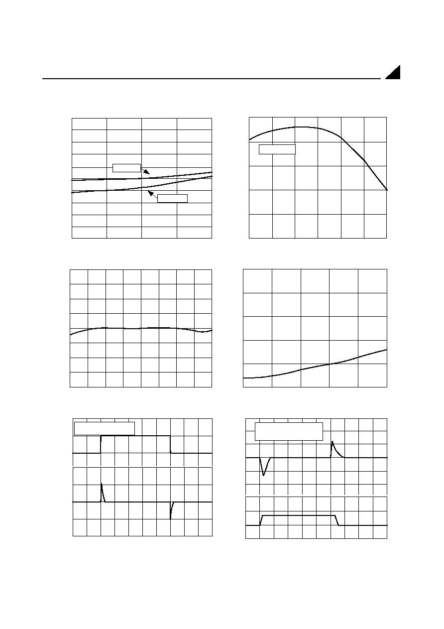
Typical Performance Characteristics
Temperature (
o
C)
Percent Change in Output Voltage vs Temperature
Output Voltage Change (%)
-50
-25
0
25
50
75
100
125
150
- 2
-1.5
- 1
-0.5
0
0. 5
1
1.5
2
Input Voltage (V)
Line Regulation
Output Voltage Deviation (%)
0
0.2
0.4
0.6
0.8
1
2
4
6
8
10
12
TIME (us)
Line Transient Response
Output Voltage Deviation (mV)
Input Voltage (V)
-40
-20
0
20
40
5.5
6.5
7.5
Cin=1uF
Cout=10uF Tantalum
0
20
40
60
80
100 120 140 160 180 200
TIME (us)
Load Transient Response
Load Current (A)
Output Voltage Deviation (mV)
0
10
20
30
40
50
60
70
80
90 100
-1
0
1
2
-20
-10
0
10
20
30
C in = 1uF
C out = 10 uF Tantalum
Preload = 100mA
Temperature (
o
C)
Load Regulation vs Temperature
Output Voltage Deviation (%)
-25
0
25
50
75
100
125
- 1
-0.80
-0.40
-0.20
0
0.20
I load=800mA
Output Current (mA)
Dropout Voltage vs Output Current
Dropout Voltage (V)
0
0. 2
0. 4
0. 6
0. 8
1. 0
1. 2
1. 4
1. 6
1. 8
2. 0
0
200
400
600
800
Tj = 125
o
C
Tj = 25
o
C
AP1117
1A Low Dropout Positive Adjustable or Fixed-Mode Regulator
Rev. A4 APR. 18, 2003
6/8
ATC
Marking Information
(1) SOT223-3L
A T C X X X
1 1 1 7
Output Type:
1117 : ADJ
17-15: 1.5V
17-18: 1.8V
17-25: 2.5V
17-33: 3.3V
17-50: 5.0V
Logo
ID Code
Month: A~L = 01~12
Year:
(Top view)
"2" = 2002
"1" = 2001
~
(2) TO252-3L
ATC
1 7- 33
Output Type:
1117: Adjustable
17-15: 1.5V
17-18: 1.8V
17-25: 2.5V
17-33: 3.3V
17-50: 5.0V
Logo
ID Code
Xth Week: 01~52
Year:
(Top view)
"02" = 2002
"01" = 2001
X X X X X
~
(3) TO220-3L
ATC
1117-33
Output Type:
1117: ADJ
1117-15: 1.5V
1117-18: 1.8V
1117-25: 2.5V
1117-33: 3.3V
1117-50: 5.0V
Logo
ID code
Year:
( Top view )
"02" = 2002
"01" = 2001
XX XX X
Xth week: 01~52
~
(4) SOT89-3L
XX
XX
1
3
2
Date Code
Month: A~L
Year: 0~9
Identification Code
( See the table )
Identification code
Output version
DA
AP1117-ADJ
DB
AP1117-1.5V
DC
AP1117-1.8V
DD
AP1117-2.5V
DE
AP1117-3.3V
DF
AP1117-5.0V
AP1117
1A Low Dropout Positive Adjustable or Fixed-Mode Regulator
Rev. A4 APR. 18, 2003
7/8
ATC
Package Dimension
(1) SOT223-3L
A
c
L
A1
SEATING PLANE
H E
K
D
B1
e
e1
B
Notes:
1. JEDEC Outline: TO-261AA
DIMENSIONS IN INCH
SYMBOL
S
MIN
NOM
MAX
A
0.059
0.065
0.071
A1
0.0008
0.002
0.003
B
0.024
0.028
0.031
B1
0.114
--
0.124(
REF)
c
0.011
0.012
0.013
D
0.248
0.256
0.264
E
0.13
0.138
0.146
e
0.09 BSC
e1
0.181 BSC
H
0.264
0.276
0.287
L
0.036
0.039
0.043
K
0.059
0.069
0.079
0°
5
o
10°
--
13
o
--
(2) TO252-3L
Variations ( Dimensions show in inch)
A
C1
C
A1
H
SEATING PLANE
SEE NOTE2
b2
E
e
b
L2
e1
D
L1
Notes:
1. JEDEC Outline: TO-252 AB
2. Mils suggested for positive contact at mounting.
DIMENSIONS IN INCH
SYMBOLS
MIN
MAX
A
0.086
0.094
A1
0.040
0.050
b
0.024 TYP.
b2
0.205
0.215
C
0.018
0.023
C1
0.018
0.023
D
0.210
0.220
E
0.250
0.265
e
0.090 BSC.
e1
0.180 BSC.
H
0.370
0.410
L
0.020
--
L1
0.025
0.040
L2
0.06
0.08
AP1117
1A Low Dropout Positive Adjustable or Fixed-Mode Regulator
Rev. A4 APR. 18, 2003
8/8
ATC
(3) TO220-3L
A
J1
F
C
SEATING PLANE
D
Q
E
L1
L
b
e
e1
b1
P
DIMENSIONS IN INCH
SYMBOLS
MIN
MAX
A
0.14
0.19
b1
0.045
0.07
b
0.02
0.045
C
0.012
0.045
D
0.56
0.65
E
0.38
0.42
e
0.09
0.11
e1
0.19
0.21
F
0.02
0.055
H1
0.23
0.27
J1
0.08
0.115
L
0.5
0.58
øP
0.139
0.161
Q
0.1
0.135
(4) SOT89
L
HE
E
D1
e1
e
A
D
b1
b
b
8
0
(2x)
c
5
0
(2x)
DIMENSIONS IN
MILLIMETER
DIMENSIONS IN
INCHES
SYMBOLS
MIN
NOM MAX
MIN
NOM MAX
A
1.40
1.50
1.60
0.055 0.059 0.063
B
0.36
0.42
0.48
0.014 0.016 0.018
b1
0.41
0.47
0.53
0.016 0.043 0.051
C
0.38
0.40
0.43
0.014 0.015 0.017
D
4.40
4.50
4.60
0.173 0.177 0.181
D1
1.40
1.60
1.75
0.055 0.062 0.069
E
2.90
3.00
3.10
0.114 0.118 0.122
e1
1.45
1.50
1.55
0.057 0.059 0.061
E
2.40
2.50
2.60
0.094 0.098 0.102
HE
3.94
------
4.25
0.155 ------ 0.167
L
0.80
------
1.20
0.031 ------ 0.047