
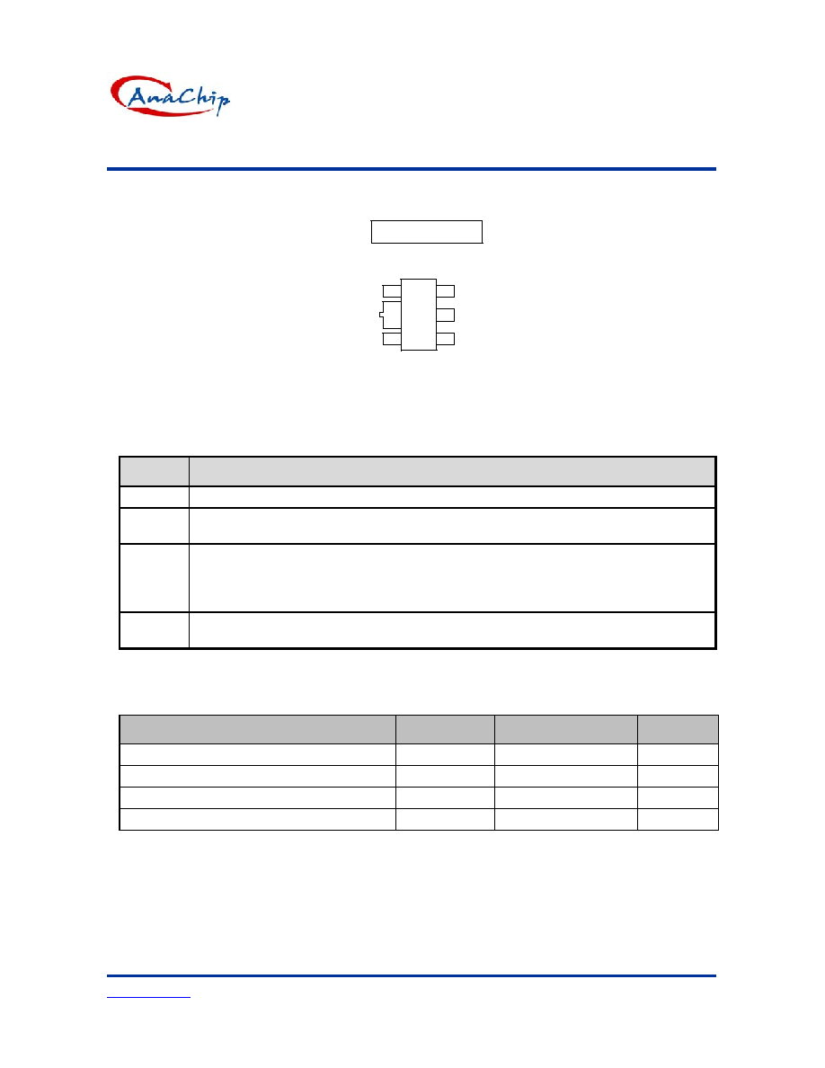
AP1119
0.5A Positive Low Dropout Fixed-Mode Regulator With EN Function
This datasheet contains new product information. Anachip Corp. reserves the rights to modify the product specification without notice. No liability is assumed as a result of the use of
this product. No rights under any patent accompany the sale of the product.
Rev. 1.0 Aug 20, 2004
1/5
Features
∑
1.3V maximum dropout at full load current
∑
Fast transient response
∑
Output current limiting
∑
Built-in thermal shutdown
∑
Packages: SOT89-5L
∑
Good noise rejection
∑
5-Terminal device with fixed 1.5V, 1.8V, 2.5V,
3.3V, 5.0V, 9.0V, 12V output.
Applications
∑
PC peripheral
∑
Communication
∑
CDROM..
General Description
AP1119 is a low dropout positive adjustable or
fixed-mode regulator with minimum of 0.5A output
current capability. The product is specifically
designed to provide well-regulated supply for low
voltage IC applications such as high-speed bus
termination and low current 3.3V logic supply.
AP1119 is also well suited for other applications
such as VGA cards. AP1119 is guaranteed to have
<1.3V dropout at full load current making it ideal to
provide well regulated fixed outputs of 1.5 to 12V
with up to 18V input supply. The AP1119 offers a
TTL ≠ Logic compatible enable pin.
Ordering Information
AP 1119 X XX X X
Low Dropout Regulator
Package
Vout
Y : SOT89-5L
15 : 1.5V
18 : 1.8V
25 : 2.5V
33 : 3.3V
50 : 5.0V
90 : 9.0V
12 : 12V
Packing
Blank : Tube
A : Taping
Lead Free
Blank : Normal
L : Lead Free Package
Typical Circuit
C2
100uF
5V
3.3V/0.5A
C1
100uF
( 5V/3.3V fixed output )
GND
Vout
Vin
1
3
2
EN
NC
4
5
OFF
ON
Tab is Vout
AP1119
0.5A Positive Low Dropout Fixed-Mode Regulator With EN
Function
Anachip Corp.
www.anachip.com.tw
Rev. 1.0 Aug 20, 2004
2/5
Connection Diagram
5 PIN SOT89
GND
Vout
Vin
1
3
2
Tab is Vout
EN
NC
4
5
Pin Descriptions
NAME
FUNCTION
GND Ground
Vout
The output of the regulator. A minimum of 10uF capacitor must be connected from this pin
to ground to insure stability.
Vin
The input pin of regulator. Typically a large storage capacitor is connected from this pin to
ground to insure that the input voltage does not sag below the minimum dropout voltage
during the load transient response. This pin must always be 1.3V higher than Vout in order
for the device to regulate properly.
EN
The input pin of regulator. TTL/CMOS compatible input Logic high = disable output, Logic
Low or open =Enable output. (internal Pull-down resistor ~ l00K).
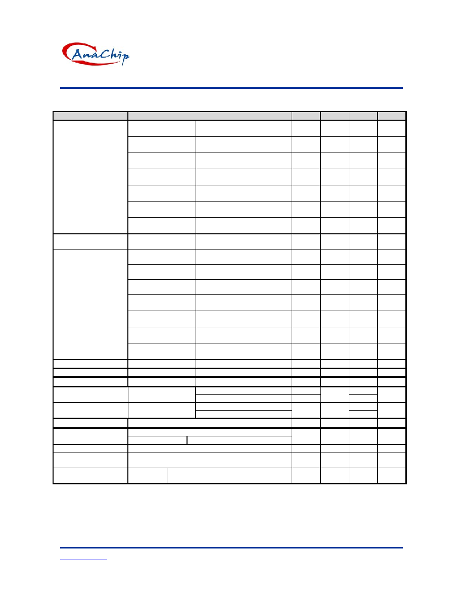
Absolute Maximum Ratings
Characteristics
Symbol
Values
Unit
DC Supply Voltage
Vin
-0.3 to 18
V
Power Dissipation
P
D
Internally
Limited
Storage Temperature
T
ST
-65 to +150
oC
Operating Junction Temperature Range
T
OP.
0 to +150
oC
AP1119
0.5A Positive Low Dropout Fixed-Mode Regulator With EN Function
Anachip Corp.
www.anachip.com.tw
Rev. 1.0 Aug 20 ,2004
3/5
Electrical Characteristics (Under Operating Conditions)
PARAMETER
CONDITIONS
MIN
TYP
MAX
UNIT
AP1119-1.5
I
OUT
= 10mA, T
J
= 25
o
C,
3VV
IN
12V
1.470
1.500 1.530 V
AP1119-1.8
I
OUT
= 10mA, T
J
= 25
o
C,
3.3VV
IN
12V
1.764
1.800 1.836 V
AP1119-2.5
I
OUT
= 10mA, T
J
= 25
o
C,
4VV
IN
12V
2.450
2.500 2.550 V
AP1119-3.3
I
OUT
= 10mA, T
J
= 25
o
C,
4.8VV
IN
12V
3.235
3.300 3.365 V
AP1119-5.0
I
OUT
= 10mA, T
J
= 25
o
C,
6.5VV
IN
12V
4.900
5.000 5.100 V
AP1119-9.0
I
OUT
= 10mA, T
J
= 25
o
C,
10.5VV
IN
18V
8.820
9.000 9.180 V
Output Voltage
AP1119-12.0
I
OUT
= 10mA, T
J
= 25
o
C,
13.5VV
IN
18V
11.760
12.000 12.240
V
Line Regulation
AP1119-XXX
I
O
=10mA,V
OUT
+1.5V<V
IN
<15V,
T
J
=25
o
C
0.2
%
AP1119-1.5
V
IN
=3V, 0mA<Io<0.5A,
T
J
=25
o
C (Note 1,2)
12 15
mV
AP1119-1.8
V
IN
=3.3V, 0mA<Io<0.5A,
T
J
=25
o
C (Note 1,2)
15 18
mV
AP1119-2.5
V
IN
=4V, 0mA<Io<0.5A,
T
J
=25
o
C (Note 1,2)
20 25
mV
AP1119-3.3
V
IN
= 5V, 0I
OUT
0.5A,
T
J
=25
o
C (Note 1,2)
26 33
mV
AP1119-5.0
V
IN
= 8V, 0I
OUT
0.5A,
T
J
=25
o
C (Note 1,2)
40 50
mV
AP1119-9.0
V
IN
=12V, 0I
OUT
0.5A,
T
J
=25
o
C (Note 1,2)
70 90
mV
Load Regulation
AP1119-12.0
V
IN
=15V, 0I
OUT
0.5A,
T
J
=25
o
C (Note 1,2)
100
120
mV
Dropout Voltage
(V
IN
-V
OUT
)
AP1119 series
I
OUT
= 0.5A ,
V
OUT
=0.1V
OUT
1.1
1.3 V
Current Limit
AP1119 series
(V
IN
-V
OUT
) = 5V
0.6
A
Minimum Load Current
AP1119-XXX
0
o
CTj125
o
C
5 10
mA
Logic Low (ON)
0.8
V
EN
Enable Input Voltage
Logic High (OFF)
2.0
V
V
EN
= 0.8V
10
I
EN
Enable Input Current
V
EN
= 2.0V
30
µA
Thermal Regulation
T
A
=25, 30ms pulse
0.008
0.04
%/W
F=120Hz,C
OUT
=25uF Tantalum, I
OUT
=0.5A
Ripple Rejection
AP1119-XXX V
IN
=V
OUT
+3V
60 70
dB
Temperature Stability
I
O
=10mA
0.5 %
JA
SOT89-5L Thermal Resistance Junction-to-Ambient(No
heat sink ;No air flow)
300
O
C/W
JC
SOT89-5L
: Control Circuitry/Power Transistor
Thermal Resistance Junction-to-Case
100
O
C/W
Note1: See thermal regulation specifications for changes in output voltage due to heating effects. Line and load regulation are
measured at a constant junction temperature by low duty cycle pulse testing. Load regulation is measured at the output lead =
1/18" from the package.
Note2: Line and load regulation are guaranteed up to the maximum power dissipation of 5W. Power dissipation is determined by the
input/output differential and the output current. Guaranteed maximum power dissipation will not be available over the full
input/output range.
Note3: Quiescent current is defined as the minimum output current required maintain regulation. At 12V input/output differential the
device is guaranteed to regulate if the output current is greater than 10mA.

AP1119
0.5A Positive Low Dropout Fixed-Mode Regulator With EN Function
Anachip Corp.
www.anachip.com.tw
Rev. 1.0 Aug 20 ,2004
4/5
Typical Performance Characteristics
Temperature (
o
C)
Percent Change in Output Voltage vs Temperature
Out
put
Volt
age C
hange (%
)
-50
-25
0
25
50
75
100
125
150
- 2
-1.5
- 1
-0.5
0
0. 5
1
1.5
2
Input Voltage (V)
Line Regulation
Out
put
Volt
age D
e
viat
ion (%
)
0
0.2
0.4
0.6
0.8
1
2
4
6
8
10
12
TIME (us)
Line Transient Response
O
u
tput Voltage Deviation (mV)
Input Voltage (V)
-40
-20
0
20
40
5.5
6.5
7.5
Cin=1uF
Cout=10uF Tantalum
0
20
40
60
80
100 120 140 160 180 200
TIME (us)
Load Transient Response
Load Current (A)
O
u
tput Voltage Deviation (mV)
0
10
20 30
40
50
60
70
80
90 100
-1
0
1
2
-20
-10
0
10
20
30
C in = 1uF
C out = 10 uF Tantalum
Preload = 100mA
Output Current (mA)
Dropout Voltage vs Output Current
D
r
opout
Volt
age (V)
0
0. 2
0. 4
0. 6
0. 8
1. 0
1. 2
1. 4
1. 6
1. 8
2. 0
0
100
200
300
400
Tj = 125
o
C
Tj = 25
o
C
Temperature (
o
C)
Load Regulation vs Temperature
Out
put
Volt
age D
e
viat
ion (%
)
-25
0
25
50
75
100
125
- 1
-0.80
-0.40
-0.20
0
0.20
I load=500mA
500
AP1119
0.5A Positive Low Dropout Fixed-Mode Regulator With EN Function
Anachip Corp.
www.anachip.com.tw
Rev. 1.0 Aug 20 ,2004
5/5
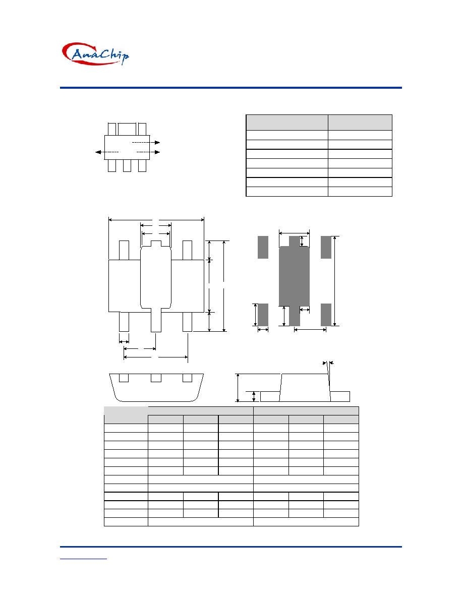
Marking Information
SOT89-5L
Date Code
Month: A~L
Year: 0~9
Identification Cod
( See the table )
1
3
2
4
5
XX
XX X
Blank: normal
L: Lead Free Package
Identification code
Output version
JF AP1119-1.5V
JG AP1119-1.8V
JH AP1119-2.5V
JI AP1119-3.3V
JJ AP1119-5.0V
JK AP1119-9.0V
JL AP1119-12V
Package Information
D
C
A
I
H
G
E
B
F
F
K
J
L
0.5
1.1
1.5
4.6
1.2
0.55
Land Pattern Recommendation (Unit: mm)
1.7
0.4
Dimensions In Millimeters
Dimensions In Inches
Symbol
Min.
Nom.
Max.
Min.
Nom.
Max.
A
4.40 4.50 4.60 0.173 0.177 0.181
B
4.05 4.15 4.25 0.159 0.163 0.167
C
1.50 1.60 1.70 0.059 0.063 0.067
D
1.30 1.40 1.50 0.051 0.055 0.059
E
2.40 2.50 2.60 0.094 0.098 0.102
F 0.80 - - 0.031 - -
G 3.00
Ref.
0.118
Ref.
H 1.50
Ref.
0.059
Ref.
I
0.40 0.46 0.52 0.016 0.018 0.020
J
1.40 1.50 1.60 0.055 0.059 0.063
K
0.35 0.39 0.43 0.014 0.015 0.017
L 5
o
Typ. 5
o
Typ.