3A Bus Terminator Regulator
AP1128
This datasheet contains new product information. Anachip Corp. reserves the rights to modify the product specification without notice. No liability is assumed as a result of the use of
this product. No rights under any patent accompany the sale of the product.
Rev.1.0 Jul 20, 2005
1/7
Features
- Ideal for DDR-I and DDR-II applications
- Capable of sourcing and sinking current 1.5A/3A
- Current limiting protection
- Thermal protection
- Current-shoot-through protection
- High accuracy output voltage at full load
- Minimum external components
- Adjustable VOUT by external resistors
- Shutdown for standby or suspend mode operation
with high-impedance output
- TO252-5 and SOP-8 Pb-free Package
Applications
- Mother Board DDR-SDRAM Termination
- Mother Board DDR-II Termination
- Game / Play Station
- Set Top Box
- PCI / AGP Graphics
- IPC
- SCSI-III Bus Termination
General Description
AP1128 is a linear regulator designed as a
cost-effective solution for active termination of DDR
SDRAM. The converting voltage range is from 1.6V
to 6V into a desired output voltage, which is
adjusted by two external resistors. The current
sourcing and sinking capability of the regulator is up
to 1.5A/3A while the output voltage within 2%/3%.
This device provides on-chip thermal shutdown and
current limit functions for circuit tolerance of the
output fault conditions. SO-8 and TO-252-5L
packages are available for all commercial and
industrial surface mount applications.
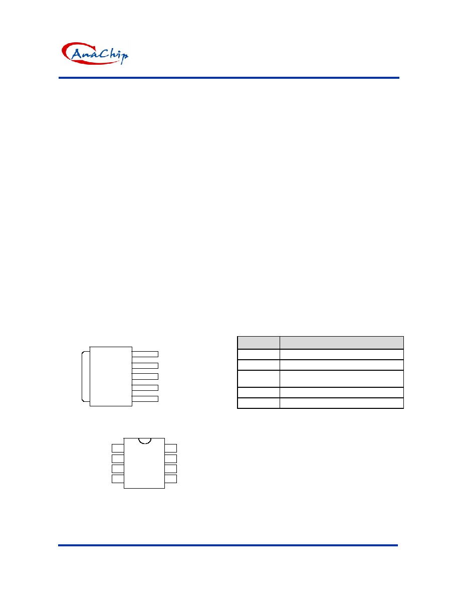
Pin Assignment
5
3
1
V
IN
V
OUT
GND
TO252-5L
( Top View )
2
4
V
CNTL(TAB)
V
REFEN
1
2
3
7
6
5
4
8
(Top View)
V
CNTL
V
CNTL
V
CNTL
V
CNTL
V
IN
GND
V
REFEN
SOP-8L
V
OUT
Pin Descriptions
Pin Name
Descriptions
V
IN
Power
Input
V
CNTL
Gate
Drive
Voltage
V
REFEN
Reference Voltage Input and Chip
Enable
GND Ground
V
OUT
Output
Voltage

3A Bus Terminator Regulator
AP1128
Anachip Corp.
www.anachip.com.tw Rev.1.0 Jul 20, 2005
2/7
Ordering Information
AP1128 X X
Package
D: TO252-5
S: SOP-8
Packing
Blank : Tube
A : Taping
Block Diagram
CNTL
V
IN
Cuurent Limiting
Sensor
V
REFEN
V
CNTL
V
OUT
GND
Thermal
Typical Circuit
C3
10uF
R2
100K
C2
1000uF
U1
AP1128
1
2
3
4
5
6
7
8
V
IN
GND
V
REFEN
V
OUT
V
CNTL
V
OUT
= 1.25V
R1
100K
C
CNTL
47uF
V
CNTL
= 3.3V
V
IN
= 2.5V
EN
C1
470uF
V
CNTL
V
CNTL
V
CNTL
Absolute Maximum Ratings
Symbol
Parameter
Rating
Unit
V
IN
Power Input Voltage
6
V
P
D
Power
Dissipation
internal
limited
HBM ESD Rating
3
KV
T
STG
Storage Temperature
-55 to 150
o
C
T
Lead
Lead Temperature (Soldering 5 sec)
260
o
C
SOP-8
(Note 3)
20
JC
Thermal
Resistance
TO252-5 6
o
C/W
SOP-8 80
JA
Thermal
Resistance
TO252-5 40
o
C/W
3A Bus Terminator Regulator
AP1128
Anachip Corp.
www.anachip.com.tw Rev.1.0 Jul 20, 2005
3/7
Electrical Characteristics
V
IN
= +2.5V, V
CNTL
= +3.3V, V
REFEN
= +1.25V, C
OUT
= 10uF (Ceramic)
Symbol
Parameter
Conditions
Min.
Typ.
Max.
Unit
V
OS
Output Offset Voltage
(Note 1)
I
OUT
=0A
-20
-5
20
mV
I
L
: 0A --> 1.5A
-
0.5
2
V
LOAD
Load Regulation
I
L
: 0A --> -1.5A
-
0.5
2
%
V
IN
Input Voltage Range (DDR I/II)
(Note2)
V
CNTL
V
IN
1.6 2.5/1.8 - V
V
CNTL
Gate Drive Voltage Range
(Note2)
V
CNTL
V
IN
- 3.3 6 V
I
CNTL
Operation Current of V
CNTL
I
OUT
= 0A
-
3
6
mA
I
SHDN
Current
in
Shutdown
V
REFEN
< 0.2V,
R
L
=180
- 10 90
uA
I
Q
Quiescent
Current
I
OUT
=0A -
1
3
mA
Short Circuit Protection
SOP-8 -
2
-
I
LIMIT
Current
Limit
TO-252 -
3
-
A
Over Temperature Protection
T
OS
Thermal
Shutdown
Temperature 3.3V
V
CNTL
5V
- 140 -
o
C
Shutdown Function
Shutdown Threshold Trigger
Output = High
0.8
-
-
Shutdown Threshold Trigger
Output = Low
-
-
0.2
V
Note 1: V
OS
is the voltage measurement V
OUT
subtracted from V
REFEN
.
Note 2: Keep V
CNTL
V
IN
at power on/off sequences.
Note 3: Surface mounted on 1 in
2
copper pad of FR4 board
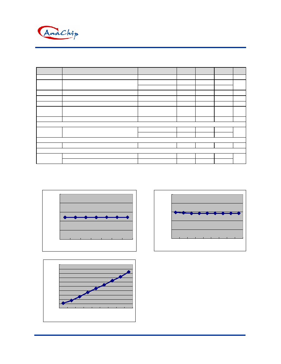
Typical Performance Characteristics
1.20
1.22
1.24
1.26
1.28
1.30
1.5
1.6
1.7
1.9
2.1
2.3
2.5
V
IN
(V)
V
OU
T
(V)
Fig 1. Line Regulation ( V
IN
v.s. V
OUT
)
1.20
1.22
1.24
1.26
1.28
1.30
2.0 2.5 3.0 3.5 4.0 4.5 5.0 5.5 6.0
V
CNTL
(V)
V
OU
T
(V
)
Fig 2. Line Regulation ( V
CNTL
v.s. V
OUT
)
0.0
0.5
1.0
1.5
2.0
2.5
3.0
3.5
4.0
4.5
5.0
2.0 2.5 3.0 3.5 4.0 4.5 5.0 5.5 6.0
V
CNTL
(V)
I
CNT
L
(mA
)
Fig 3. Line Regulation ( V
CNTL
v.s. I
CNTL
)

3A Bus Terminator Regulator
AP1128
Anachip Corp.
www.anachip.com.tw Rev.1.0 Jul 20, 2005
4/7
Typical Performance Characteristics (Continued)
Fig 4. Output Short-Circuit Protection
Fig 5. Output Short-Circuit Protection
V
IN
=2.5V, V
CNTL
=3.3V, V
REFER
=1.25V, Temp(IC Body) = 98
o
C
Fig 7. Transient Response
V
IN
=1.8V, V
CNTL
=3.3V, V
REFER
=0.9V
Fig 8. Transient Response
-1.5A
Output Transient Voltage
V
REFER
=1.25V
Output Current
1.5A
-1.5A
Output Transient Voltage
V
REFER
=0.9V
Output Current
1.5A

3A Bus Terminator Regulator
AP1128
Anachip Corp.
www.anachip.com.tw Rev.1.0 Jul 20, 2005
5/7
Typical Performance Characteristics (Continued)
Fig 9. Safe Operating Area
Marking Information
1128
Part Number
Logo
ID Code
Xth Week: 01~52
Year:
(Top View)
"02" = 2002
"01" = 2001
X X X X X
~
(TO252-5)
8
5
1
4
( Top View )
Logo
Part No.
ID code: internal
Year: "01" =2001
"02" =2002
Xth week: 01~52
~
AP1128
YY WW X
(SOP-8)