 | –≠–ª–µ–∫—Ç—Ä–æ–Ω–Ω—ã–π –∫–æ–º–ø–æ–Ω–µ–Ω—Ç: AP13825W | –°–∫–∞—á–∞—Ç—å:  PDF PDF  ZIP ZIP |
AP138
300mA Low-Noise CMOS LDO
This datasheet contains new product information. Anachip Corp. reserves the rights to modify the product specification without notice. No liability is assumed as a result of the use of
this product. No rights under any patent accompany the sale of the product.
Rev. 1.0 Oct 29, 2004
1/7
Features
- Very low dropout voltage
- Low current consumption: Typ.30µA, Max. 35µA
- Output voltage: 1.8V, 2.5V, 2.8V, 3.0V and 3.3V
- High accuracy output voltage:
±1.5%
- Guaranteed 300mA output
- Input range up to 7.0V
- Thermal shutdown
- Current limiting
- Stability with low ESR capacitors
- Factory pre-set output voltages
- Low temperature coefficient
- Pb-free package: SOT23-5L
Applications
- Battery-powered devices
- Personal communication devices
- Home electric/electronic appliances
- PC peripherals
General Descriptions
The AP138 is a positive voltage linear regulator
utilizing CMOS technology. The features that
include low quiescent current (30µA typ.), low
dropout voltage, and high output voltage accuracy,
make it ideal for battery applications. EN input
connected to CMOS has low bias current. The
space-saving SOT23-5L package is attractive for
"Pocket" and "Hand Held" applications.
This rugged device has both thermal shutdown, and
current limit protections to prevent device failure
under the "Worst" operating conditions.
In a low noise, regulated supply application, a
1000pF capacitor is necessary to be placed in
between Bypass and Ground.
The AP138 is stable with a low ESR output
capacitor of 1.0µF or greater.
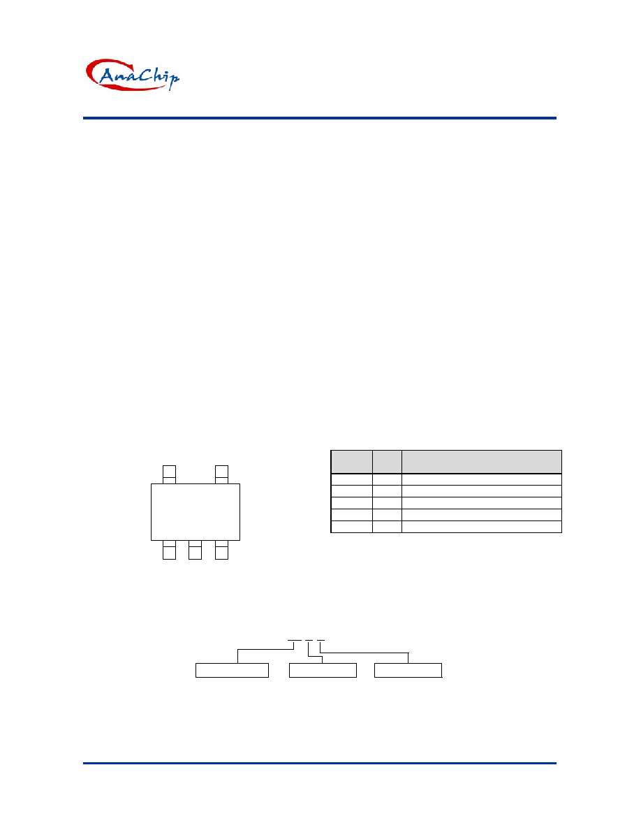
Pin Assignments
1
3
2
5
4
BYP
V
IN
EN
GND
V
OUT
AP138
SOT23-5
(Top View)
Pin Descriptions
Pin
Name
Pin
No.
Function
V
IN
1
Power
Supply
GND 2 Ground
EN 3
Enable
Pin
BYP 4 Bypass
Signal
Pin
V
OUT
5 Output
Ordering Information
AP138 XX X X
W : SOT23-5L
Output voltage
Package
18: 1.8V
25: 2.5V
28: 2.8V
30: 3.0V
33: 3.3V
Blank: Tube
A: Taping
Packing
AP138
300mA Low-Noise CMOS LDO
Anachip Corp.
www.anachip.com.tw Rev. 1.0 Oct 29, 2004
2/7
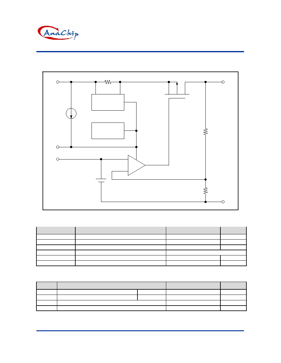
Block Diagram
Current
Limit
Thermal
Shutdown
AMP
+
-
Vref
BYP
EN
1uA
V
OUT
GND
V
IN
R1
R2
Absolute Maximum Ratings
Symbol
Parameter
Rating
Unit
V
CC
Input
Voltage
+7
V
I
OUT
Output
Current
P
D
/ (V
IN
-V
O
) mA
V
OUT
Output Voltage
GND - 0.3 to V
IN
+ 0.3
V
ESD
Classification
B
T
A
Ambient Temperature Range
-40 to +85
∫C
T
J
Junction Temperature Range
-40 to +125
∫C
Thermal Information
Symbol
Parameter
Maximum
Unit
jc
Thermal
Resistance
SOT23-5L 160 ∫C/W
P
D
Internal Power Dissipation (
T=100 ∫C) SOT23-5L 250 mW
T
J
Maximum
Junction
Temperature
150
∫C
T
Lead
Maximum Lead Temperature (10 sec)
300
∫C

AP138
300mA Low-Noise CMOS LDO
Anachip Corp.
www.anachip.com.tw Rev. 1.0 Oct 29, 2004
3/7
Electrical Characteristics
(T
A
=+25∫C, unless otherwise noted.)
Symbol
Parameter
Test Conditions
Min.
Typ.
Max.
Unit
V
IN
Input
Voltage
Note 1
- 7 V
V
OUT
Output
Voltage
Accuracy
I
O
=1mA to 300mA
-1.5
-
1.5
%
1.2V<V
O(NOM)
2.0V
- -
1300
2.0V<V
O(NOM)
2.5V
- -
800
V
DROPOUT
Dropout Voltage
I
O
=1mA to 300mA,
V
OUT
=V
O(NOM)
-1.5%
2.5V<V
O(NOM)
- -
300
mV
I
OUT
Output
Current
V
OUT
> 1.2V
300
-
-
mA
I
LIMIT
Current
Limit
V
OUT
> 1.2V
300
450
-
mA
I
Q
Quiescent
Current
I
O
=0mA -
30
35
µA
I
GND
Ground Pin Current
I
O
=1mA to 300mA
-
30
50
µA
REG
LINE
Line Regulation
I
OUT
=5mA, V
IN
=V
OUT
+1 to V
OUT
+2 -0.1
0.02
0.1
%
REG
LOAD
Load Regulation
I
O
=1mA to 300mA
-
0.2
1
%
OTS
Over Temperature
Shutdown
- 150 -
o
C
OTH
Over Temperature
Hysteresis
-
30
-
o
C
TC
V
OUT
Temperature
Coefficient
-
40
-
ppm/
o
C
f=1KHz -
60
-
f=10KHz -
50
-
PSRR Power Supply Rejection
I
O
=100mA,
C
O
=2.2µF ceramic
f=100KHz - 40 -
dB
f=1KHz -
75
-
f=10KHz -
55
-
PSRR Power Supply Rejection
I
O
=100mA,
C
O
=2.2µF ceramic,
C
BYP
=0.01µF
f=100KHz - 30 -
dB
C
O
=2.2uF - 30 -
eN Output
Voltage
Noise
f=10Hz to 100kHz,
I
O
=10mA, C
BYP
=0µF
C
O
=100uF - 20 -
µVrms
C
O
=2.2uF - 30 -
eN Output
Voltage
Noise
f=10Hz to 100kHz,
I
O
=10mA, C
BYP
=0.01µF C
O
=100uF - 20 -
µVrms
I
SD
Shutdown Supply
Current
V
IN
=5.0V, V
OUT
=0V, V
EN
< V
EL
-
2.0
3.0
µA
I
EH
V
EN
=V
IN
, V
IN
=2.6V to 7V
-
-
0.1
µA
I
EL
EN Input Bias Current
V
EN
=0V, V
IN
=2.6V to 7V
-
2.0
3.0
µA
V
EH
V
IN
=2.6V to 7V
2
-
V
IN
V
V
EL
EN Input Threshold
V
IN
=2.6V to 7V
0
-
0.4
V
Note 1. : V
IN(MIN)
=V
OUT
+V
DROPOUT
Typical Application
AP138
BYP
EN
V
OUT
GND
V
IN
C1
1uF
C2
1nF
C3
1uF
IN
OUT
AP138
300mA Low-Noise CMOS LDO
Anachip Corp.
www.anachip.com.tw Rev. 1.0 Oct 29, 2004
4/7
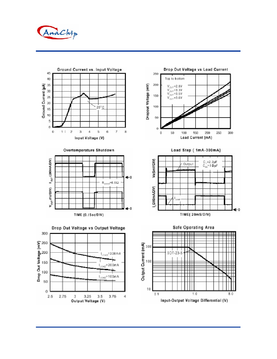
Typical Performance Characteristics
AP138
300mA Low-Noise CMOS LDO
Anachip Corp.
www.anachip.com.tw Rev. 1.0 Oct 29, 2004
5/7
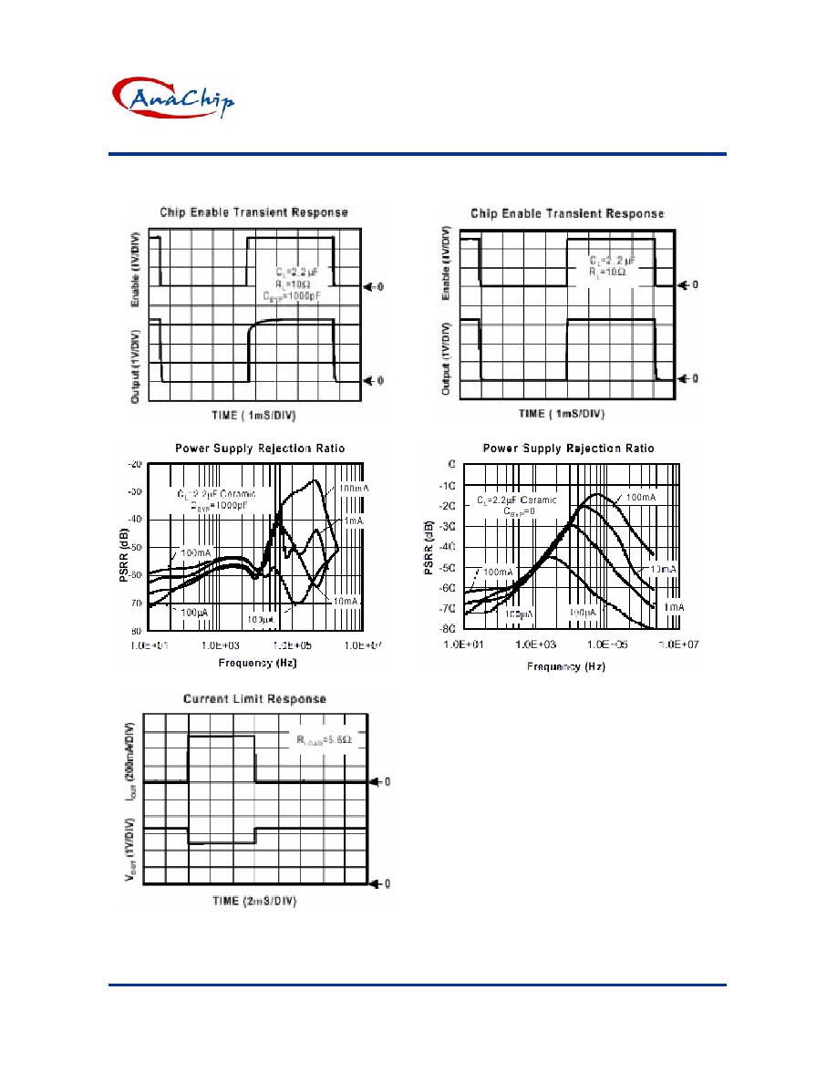
Typical Performance Characteristics (Continued)