
AP1537
PWM Control 3A Step-Down Converter
This datasheet contains new product information. Anachip Corp. reserves the rights to modify the product specification without notice. No liability is assumed as a result of the use of
this product. No rights under any patent accompany the sale of the product.
Rev. 1. 3 May 09, 2006
1/7
Features
- Input voltage: 3.6V to 18V.
- Output voltage: 0.8V to V
CC
.
- Duty ratio: 0% to 100% PWM control
- Oscillation frequency: 500KHz typ.
- Soft-start, Current Limit, Enable function
- Thermal Shutdown function
- Built-in internal SW P-channel MOS
- Low ESR output capacitor (Multi-layer chip
capacitor (MLCC)) application
- SOP-8L Pb-Free Package.
Applications
- PC Motherboard
- LCD Monitor
- Graphic Card
- DVD-Video Player
- Telecom Equipment
- ADSL Modem
- Printer and other Peripheral Equipment
- Microprocessor core supply
- Networking power supply
General Description
AP1537 consists of step-down switching regulator
with PWM control. These devices include a reference
voltage source, oscillation circuit, error amplifier,
internal PMOS and etc.
AP1537 provides low-ripple power, high efficiency,
and excellent transient characteristics. The PWM
control circuit is able to vary the duty ratio linearly
from 0 up to 100%. This converter also contains an
error amplifier circuit as well as a soft-start circuit that
prevents overshoot at startup. An enable function,
an over current protect function and a short circuit
protect function are built inside, and when OCP or
SCP happens, the operation frequency will be
reduced from 500KHz to 50KHz. Also, an internal
compensation block is built in to minimum external
component count.
With the addition of an internal P-channel Power MOS,
a coil, capacitors, and a diode connected externally,
these ICs can function as step-down switching
regulators. They serve as ideal power supply units for
portable devices when coupled with the SOP�8L
mini-package, providing such outstanding features as
low current consumption. Since this converter can
accommodate an input voltage up to 18V, it is also
suitable for the operation via an AC adapter.
Pin Assignments
)
1
2
3
4
8
7
6
5
FB
Output
Comp
AP1537
Output
EN
Vss
Vss
V
CC
Pin Descriptions
Name
Pin
Description
FB 1
Feedback
pin
EN
2
Power-off pin
H: Normal operation
(Step-down operation)
L: Step-down operation stopped
(All circuits deactivated)
Comp
3 Compensation
pin
V
CC
4
IC power supply pin
Output
56
Switch Pin. Connect external
inductor/diode here. Minimize trace
area at this pin to reduce EMI.
V
SS
78 GND Pin

AP1537
PWM Control 3A Step-Down Converter
Anachip Corp.
www.anachip.com.tw Rev. 1.3 May 09, 2006
2/7
Ordering Information
AP 1537 X X
Package
Packing
S: SOP-8L
Blank : Tube
A : Taping
Block Diagram
Oscillation
Circuit
Reference Voltage
Source with Soft Start
PWM-Switched
Control Circuit
+
-
Vss
V
EN
EN
100uA
Comp
FB
Vcc
Thermal
Shutdown
Output
Absolute Maximum Ratings
Symbol
Parameter
Rating
Unit
V
CC
*1
V
CC
Pin Voltage
V
SS
- 0.3 to V
SS
+ 20
V
V
FB
Feedback Pin Voltage
V
SS
- 0.3 to V
CC
V
V
EN
EN Pin Voltage
V
SS
- 0.3 to V
IN
+ 0.3
V
V
OUTPUT
Switch
Pin
Voltage
V
SS
- 0.3 to V
IN
+ 0.3
V
P
D
Power Dissipation
1000
mW
T
OPR
Junction Operating Temperature Range
-20 to +125
o
C
T
STG
Storage Temperature Range
-40 to +150
o
C
JC
Thermal Resistance Junction-to-Case
3 inch
2
Copper as a heat-sink
15
o
C/W
JA
Thermal Resistance Junction-to-Case
3 inch
2
Copper as a heat-sink
65
o
C/W
Caution: The absolute maximum ratings are rated values exceeding which the product could suffer physical damage. These values must
therefore not be exceeded under any conditions.
AP1537
PWM Control 3A Step-Down Converter
Anachip Corp.
www.anachip.com.tw Rev. 1.3 May 09, 2006
3/7
Electrical Characteristics
(V
IN
= 12V, T
a
=25
�C
, unless otherwise specified)
Symbol
Parameter
Conditions
Min.
Typ.
Max.
Unit
V
IN
Input
Voltage
--
3.6
-
18 V
V
FB
Feedback
Voltage
I
OUT
=0.1A 0.784
0.8
0.816
V
I
FB
Feedback
Bias
Current I
OUT
=0.1A -
0.1
0.5
�A
I
SW
Switch
Current
--
3.5
-
-
A
I
SSS
Current Consumption
During Power Off
V
EN
=0V
-
10
-
�A
V
OUT
/V
OUT
Line Regulation
V
IN
= 5V~18V, I
OUT
=0.2A -
1
2
%
V
OUT
/V
OUT
Load Regulation
I
OUT
= 0.1 to 3A
-
0.2
0.5
%
f
OSC
Oscillation Frequency
Measure waveform at SW pin
400
500
600
KHz
f
OSC1
Frequency of Current Limit
or Short Circuit Protect
Measure waveform at SW pin
40
-
-
KHz
V
SH
Evaluate oscillation at SW pin
2.0
-
-
V
SL
EN Pin Input Voltage
Evaluate oscillation stop at SW pin
-
-
0.8
V
I
SH
V
IN
= 12V
-10
-
10
�A
I
SL
EN Pin Input Leakage
Current
-- -10
-
10
�A
T
SS
Soft-Start
Time
--
0.3
2
5 ms
V
IN
=5V, V
FB
=0V -
110
150
R
DSON
Internal MOSFET Rdson
V
IN
=12V, V
FB
=0V -
70
100
m
EFFI Efficiency
V
IN
= 12V, V
OUT
= 5V
I
OUT
= 3A
- 91 - %
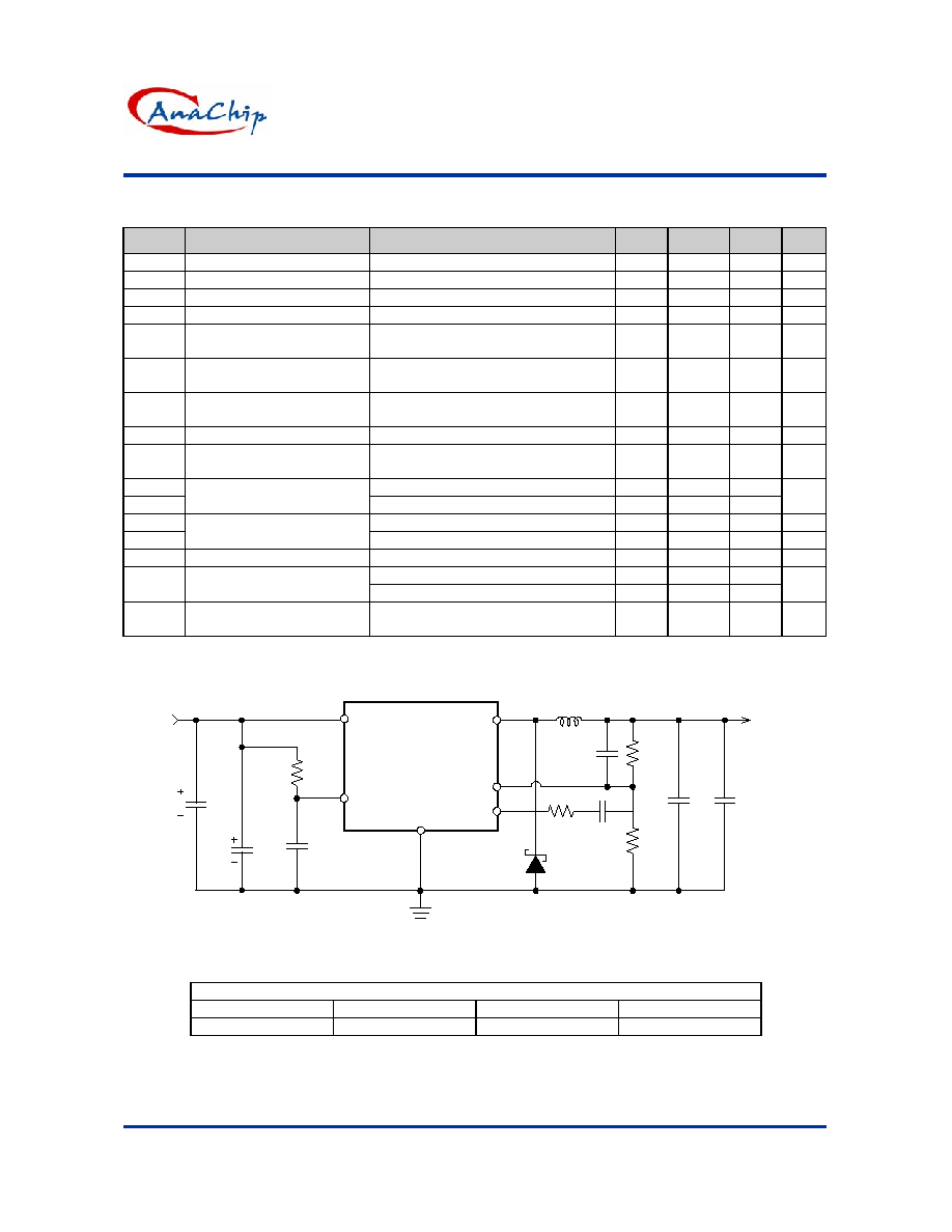
Typical Application Circuit
AP1537
+
-
V
SS
EN
C
C
R
A
R
B
D1
FB
Vcc
Output
CVcc
V
OUT
V
IN
C
OUT
C
IN
10nF
C
EN
R
EN
100K
Note: V
OUT
= V
FB
x (1+R
A
/R
B
)
R
B
=0.7K~5K ohm
L1
22uH
6.8K
1.3K
0.1uF
+
-
C
0.1uF
33uF
22uF
0.1uF
=5V
Comp
1K 1800pF
V
IN
=12V, I
MAX
=3A
V
OUT
2.5V 3.3V 5V
L1 Value
18uH 22uH 22uH

AP1537
PWM Control 3A Step-Down Converter
Anachip Corp.
www.anachip.com.tw Rev. 1.3 May 09, 2006
4/7
Typical Performance Characteristics
AP1537 Vin v.s. Frequency
(Vout=3.3V; Iout=0.2A)
400
405
410
415
420
425
430
435
440
445
450
0
5
10
15
20
Vin (V)
Fosc
(KHz)
AP1537 Vin v.s. FB
(Vout=3.3V; Iout=0.2A)
0.74
0.75
0.76
0.77
0.78
0.79
0.80
0.81
0.82
0.83
0.84
0
5
10
15
20
Vin (V)
FB (
V
)
AP1537 Line Regulation
( Iout=0.2A)
3.10
3.15
3.20
3.25
3.30
3.35
3.40
0
5
10
15
20
Vin(V)
Vout
(V)
5.00
5.01
5.02
5.03
5.04
5.05
5.06
5.07
5.08
5.09
5.10
0.0
1.0
2.0
3.0
Iout (A)
Vout (A)
AP1537 Load Regulation
(Vin=12V)
AP1537 Efficiency
0
10
20
30
40
50
60
70
80
90
100
0.0
1.0
2.0
3.0
Iout (A)
E
f
fi
ci
e
n
c
y (
%
)
Vout:5.0V
Vout:3.3V

AP1537
PWM Control 3A Step-Down Converter
Anachip Corp.
www.anachip.com.tw Rev. 1.3 May 09, 2006
5/7
Typical Performance Characteristics (Continued)
AP1537 Vout Ripple
(Vin=12V; Vout=5V; Iout=0.2A)
AP1537 Vout Ripple
(Vin=12V; Vout=5V; Iout=3A)
Test Circuit
A
FB
VCC
VSS
EN
open
open
OUTPUT
Comp
open
FB
VCC
VSS
EN
+
-
Osc
i
l
l
a
t
io
n
OUTPUT
A
Comp
FB
VCC
VSS
EN
+
-
+
-
V
OUTPUT
Comp
Operation function test
Feedback function test
Enable function test