
AP2003
Synchronous PWM Controller
(Preliminary)
This datasheet contains new product information. Anachip Corp. reserves the rights to modify the product specification without notice. No liability is assumed as a result of the use of
this product. No rights under any patent accompany the sale of the product.
Rev. 0.1 Feb.10, 2004
1/6
Features
- Single or Dual Supply Application
- 0.8V + 1.0% Voltage Reference.
- Fast transient response.
- Synchronous operation for high efficiency (95%)
- Soft Start functions
- Small size with minimum external components
- Industrial temperature range
- Under Voltage Lockout function
- SOP-8L package
Applications
- Microprocessor core supply
- Low cost synchronous applications
- Voltage Regulator Modules (VRM)
- DDR termination supplies
- Networking power supplies
- Sequenced power supplies
General Description
The AP2003 is a low-cost, full featured, and
synchronous voltage-mode controller designed for
use in single ended power supply applications
where efficiency is of the primary concern. This
synchronous operation allows the elimination of
heat sinks in many applications. The AP2003 is
ideal for implementing DC/DC converters needed to
power advanced microprocessors in low cost
systems, or in distributed power applications where
efficiency is important. Internal level-shift,
high-side drive circuitry, and preset shoot-thru
control, allows the use of inexpensive N-channel
power switches.
AP2003 features include temperature compensated
voltage reference, an internal 200KHz virtual
frequency oscillator, under-voltage lockout
protection, soft-start, and shutdown function.
Pin Assignment
SOP-8L
1
2
3
4
5
6
7
8
(Top View)
VCC
GND
AP2003
DRVH
DRVL
BSTH
SENSE
SS/SHDN
COMP
Ordering Information
AP2003 X X X
Package
Packing
S: SOP-8L
Blank : Tube
A : Taping
Lead Free
Blank : Normal
L : Lead Free Package
Pin Descriptions
Name
Description
VCC Chip
supply
voltage
DRVH
High side driver output
DRVL
Low side driver output
BSTH
Bootstrap, high side driver
SENSE
Voltage sense input
COMP Compensation
pin
SS/
SHDN
Soft start, a capacitor to ground sets
the slow start time
GND Ground

AP2003
Synchronous PWM Controller
(Preliminary)
Anachip Corp.
www.anachip.com.tw Rev. 0.1 Feb.10, 2004
2/6
Block Diagram
DRVH
DRVL
VCC
GND
SS/SHDN
SENSE
BSTH
DRVH
DRVL
+
-
+
-
+
-
+
-
One-Shot
Oscillator
PWM
Foult
Ob
S
R
0.6V
0.5V
Vcc
10uA
2uA
Error Amp
Under
Voltage
Vbg
0.8V
COMP
Cross
Current
Control
Absolute Maximum Ratings
Symbol
Parameter
Max.
Unit
V
IN
VCC to GND
-1 to 14
V
JC
Thermal Resistance Junction to Case
60
o
C/W
JA
Thermal Resistance Junction to Ambient
160
o
C/W
T
OP
Operating Temperature Range
-40 to +85
o
C
T
ST
Storage Temperature Range
-65 to +150
o
C
T
LEAD
Lead Temperature (Soldering) 10 Sec.
300
o
C

AP2003
Synchronous PWM Controller
(Preliminary)
Anachip Corp.
www.anachip.com.tw Rev. 0.1 Feb.10, 2004
3/6
Electrical Characteristics
Unless specified: V
CC
= 12V; GND = 0V; FB = V
O
; V
BSTH-GND
= 12V; T
J
= 25
o
C
Symbol
Parameter
Conditions
Min.
Typ.
Max.
Unit
Power Supply
V
CC
Supply
Voltage
V
CC
4.2
16
V
I
CC
Supply
Current
6 10 mA
V
LINE
Line Regulation
VO = 2.5V
0.5
%
Error Amplifier
A
OL
Gain
(A
OL
)
50 dB
I
B
Input
Bias
5 8 uA
Oscillator
F
OSC
Oscillator
Frequency
180 200 220 KHz
DC
MAX
Oscillator Max Duty Cycle
90
95
%
Mofset Drivers
I
DRVH
DRVH
Source/Sink
V
BSTH
� V
DRVH
=4.5V
V
DRVH
� V
PHASE
= 2V
1 A
I
DRVL
DRVL
Source/Sink
V
BSTH
� V
DRVL
= 4.5V
V
DRVL
� V
GND
= 2V
1 A
Protection
T
DEAD
Dead
Time
45 100 nS
Reference
Reference
Voltage
0.792 0.8 0.808 V
V
REF
Accuracy
0
o
C to 70
o
C
-1 +
1
%
Soft Start
I
SSC
Charge
Current
V
SS
= 1.5V
8.0
10
12
uA
I
SSD
Discharge
Current
V
SS
= 1.5V
1.3
2
2.7
uA
Under voltage lockout (UVLO)
V
UT
Upper threshold voltage
(V
CC
)
4.2 V
V
LWT
Lower threshold voltage
(V
CC
)
4.1 V
V
HT
Hysteresis
(V
CC
)
I
O(REF)
= 0.1mA
T
A
= 25�C
200 mV
Note 1. Specification refers to Typical Application Circuit.
Note 2. This device is ESD sensitive. Use of standard ESD handling precautions is required.
AP2003
Synchronous PWM Controller
(Preliminary)
Anachip Corp.
www.anachip.com.tw Rev. 0.1 Feb.10, 2004
4/6
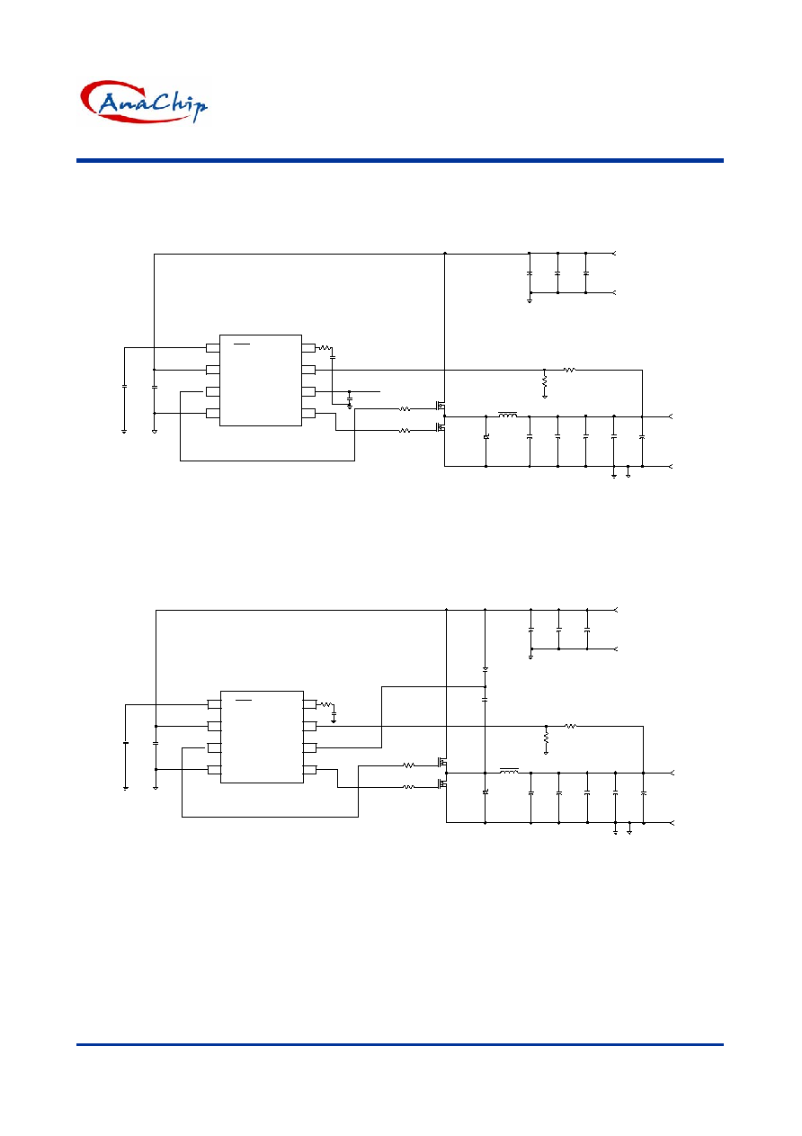
Typical Application Circuit
(1)
8
7
6
5
1
2
3
4
D1
Option
VCC
COMP
SS/SHDN
SENSE
DRVH
BSTH
GND
DRVL
Q1
STP40NE
Q2
STP40NE
L1
4uH
C9
180/4V
C10
180/4V
C11
180/4V
C12
180/4V
C13
180/4V
Vout=2.0V*
+
-
Vin
5V
+
-
C8
680/6.3V
C7
680/6.3V
C6
680/6.3V
R7
127
R8
191*
Note:
* Vout=0.8 x (1+R8/R7)
+12V
AP2003
C5
10u
C2
0.1u
R6 Option
R5 Option
(2)
8
7
6
5
1
2
3
4
D1
Option
VCC
COMP
SS/SHDN
SENSE
DRVH
BSTH
GND
DRVL
Q1
STP40NE
Q2
STP40NE
L1
4uH
C9
180/4V
C10
180/4V
C11
180/4V
C12
180/4V
C13
180/4V
Vout=2.0V*
+
-
Vin
5V
+
-
C8
680/6.3V
C7
680/6.3V
C6
680/6.3V
R7
127
R8
191*
Note:
* Vout=0.8 x (1+R8/R7)
AP2003
C5
10u
C2
0.1u
R5 Option
C1
1u
5V input with Bootstrapped BSTH
R6 Option
D2

AP2003
Synchronous PWM Controller
(Preliminary)
Anachip Corp.
www.anachip.com.tw Rev. 0.1 Feb.10, 2004
5/6
Function Description
Synchronous Buck Converter
Primary V
CORE
power is provided by a synchronous,
voltage-mode pulse width modulated (PWM)
controller. This section has all the features required
to build a high efficiency synchronous buck
converter, shutdown function.
The output voltage of the synchronous converter is
set and controlled by the output of the error
amplifier. The external resistive divider reference
voltage is derived from an internal trimmed
band-gap voltage reference. The inverting input of
the error amplifier receives its voltage from the
SENSE pin.
The internal oscillator uses an on-chip capacitor
and trimmed precision current sources to set the
oscillation frequency to 200KHz. The triangular
output of the oscillator sets the reference voltage at
the inverting input of the comparator. When the
oscillator output voltage drops below the error
amplifier output voltage, the comparator output
goes high. This pulls DRVL low, turning off the
low-side FET, and DRVH is pulled high, turning on
the high-side FET (once the cross-current control
allows it). When the oscillator voltage rises back
above the error amplifier output voltage, the
comparator output goes low. This pulls DRVH low,
turning off the high-side FET, and DRVL is pulled
high, turning on the low-side FET (once the
cross-current control allows it).
As SENSE increases, the output voltage of the
error amplifier decreases. This causes a reduction
in the on-time of the high-side MOSFET connected
to DRVH, hence lowering the output voltage.
Under Voltage Lockout
The under voltage lockout circuit of the AP2003
assures that the high-side MOSFET driver outputs
remain in the off state whenever the supply voltage
drops below set parameters. Lockout occurs if V
CC
falls below 4.1V. Normal operation resumes once
V
CC
rises above 4.2V.
Soft Start
Initially, SS/
SHDN
sources 10uA of current to
charge an external capacitor. The outputs of the
error amplifiers are clamped to a voltage
proportional to the voltage on SS/
SHDN
. This
limits the on-time of the high-side MOSFETs, thus
leading to a controlled ramp-up of the output
voltages.
Hiccup Mode
During power up, the SS/
SHDN
pin is internally
pulled low until V
CC
reaches the under-voltage
lockout level of 4.2V. Once V
CC
has reached 4.2V,
the SS/
SHDN
pin is released and begins to source
10uA of current to the external soft-start capacitor.
As the soft-start voltage rises, the output of the
internal error amplifier is clamped to this voltage.
When the error signal reaches the level of the
internal triangular oscillator, which swings from 1V
to 2V at a fixed frequency of 200KHz, switching
occurs. As the error signal crosses over the
oscillator signal, the duty cycle of the PWM signal
continues to increase until the output comes into
regulation.
The soft-start voltage will begin to decrease as the
2uA of current discharge the external capacitor.
When the soft-start voltage reaches 0.8V, the
SS/
SHDN
pin will begin to source 10uA and begin
to charge the external capacitor causing the
soft-start voltage to rise again. Again, when the
soft-start voltage reaches the level of the internal
oscillator, switching will occur.
In conclusion, above is shown a typical "12V
Application Circuit" which has a BSTH voltage
derived by bootstrapping input voltage to the
PHASE node through diode D2. This circuit is very
useful in cases where only single input power of
5V(or 12V) is available.
In order to prevent substrate glitching, a
small-signal diode should be placed in close
proximity to the chip with cathode connected to
PHASE and anode connected to GND.