
AP2014/A
Synchronous PWM Controller
This datasheet contains new product information. Anachip Corp. reserves the rights to modify the product specification without notice. No liability is assumed as a result of the use of this
product. No rights under any patent accompany the sale of the product.
Rev. 1.2 Nov 29, 2005
1/12
Features
- Synchronous Controller in 8-Pin Package
- Operating with single 5V or 12V supply voltage
- Internal 200KHz Oscillator (400KHz for AP2014A)
- Soft-Start Function
- Fixed Frequency Voltage Mode
- 500mA Peak Output Drive Capability
- Protects the output when control FET is shorted
- SOP-8L/PDIP-8L Pb-Free package
Applications
- Graphic Card
- Hard Disk Drive
- DDR memory source sink Vtt application
- Low cost on-board DC to DC such as 5V to 3.3V,
2.5V or 1.8V
Pin Assignments
SOP-8L/PDIP-8L
1
2
3
4
5
6
7
8
(Top View)
Vcc
GND
AP2014/A
LDrv
HDrv
Vc
Comp
FB
SS
General Description
The AP2014 controller IC is designed to provide a
low cost synchronous Buck regulator for on-board
DC to DC converter applications. With the migration
of today's ASIC products requiring low supply
voltages such as 1.8V and lower, together with
currents in excess of 3A, traditional linear regulators
are simply too lossy to be used when input supply is
5V or even in some cases with 3.3V input supply.
The AP2014 together with dual N-channel
MOSFETs such as AF9410, provide a low cost
solution for such applications. This device features
an internal 200KHz oscillator (400KHz for "A"
version), under-voltage lockout for both Vcc and Vc
supplies, an external programmable soft-start
function as well as output under-voltage detection
that latches off the device when an output short is
detected.
Pin Descriptions
Pin
Name
Pin
No.
Description
FB 1
This pin is connected directly to the output of the
switching regulator via resistor divider to provide
feedback to the Error amplifier.
Vcc 2
This pin provides biasing for the internal blocks of
the IC as well as power for the low side driver. A
minimum of 1uF, high frequency capacitor must be
connected from this pin to ground to provide peak
drive current capability.
LDrv
3
Output driver for the synchronous power MOSFET.
GND 4
This pin serves as the ground pin and must be
connected directly to the ground plane. A high
frequency capacitor (0.1 to 1uF) must be connected
from V5 and V12 pins to this pin for noise free
operation.
HDrv
5
Output driver for the high side power MOSFET.
Vc 6
This pin is connected to a voltage that must be at
least 4V higher than the bus voltage of the switcher
(assuming 5V threshold MOSFET) and powers the
high side output driver. A minimum of 1uF, high
frequency capacitor must be connected from this
pin to ground to provide peak drive current
capability.
Comp
7
Compensation pin of the error amplifier. An external
resistor and capacitor network is typically connected
from this pin to ground to provide loop
compensation.
SS 8
This pin provides soft-start for the switching
regulator. An internal current source charges an
external capacitor that is connected from this pin to
ground which ramps up the output of the switching
regulator, preventing it from overshooting as well as
limiting the input current. The converter can be
shutdown by pulling this pin below 0.5V.

AP2014/A
Synchronous PWM Controller
Anachip Corp
www.anachip.com.tw Rev. 1.2 Nov 29, 2005
2/12
Ordering Information
AP2014/A X
X
Package
Packing
S: SOP-8L
N: PDIP-8L
Blank : Tube
A : Taping
Block Diagram
SS
Fb
Comp
GND
LDrv
Vcc
HDrv
Vc
25K
25K
1.25V
POR
20uA
64uA
Max
3V
Error Amp
+
-
Oscillator
Ct
Error Comp
+
-
S
R
Q
Reset Dom
4
3
2
5
6
7
1
8
+
-
+
-
Bias
Generator
Vcc
4.0V
Vc
3.5V
0.2V
0.2V
3V
1.25V
POR
+
-
FbLo Comp
0.5V
POR
Absolute Maximum Ratings
Symbol
Parameter
Range.
Unit
V
CC
Vcc Supply Voltage
20
V
V
C
Vc Supply Voltage (not rated for inductive load)
32
V
T
ST
Storage Temperature Range
-65 to 150
o
C
T
J
Operating Junction Temperature Range
0 to 125
o
C
JC
Thermal Resistance Junction to Case
90
o
C/W
JA
Thermal Resistance Junction to Ambient
250
o
C/W
AP2014/A
Synchronous PWM Controller
Anachip Corp
www.anachip.com.tw Rev. 1.2 Nov 29, 2005
3/12
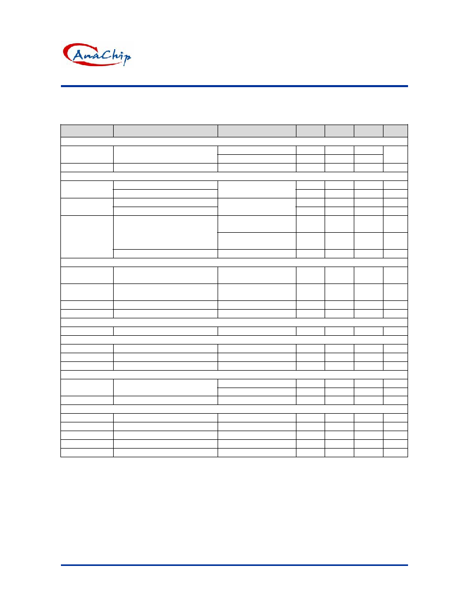
Electrical Characteristics
Unless otherwise specified, these specifications apply over V
CC
=5V, V
C
=12V and T
A
=0 to 70�C. Typical values refer to T
A
=25�C. Low duty
cycle pulse testing is used which keeps junction and case temperatures equal to the ambient temperature.
Symbol
Parameter
Conditions
Min.
Typ.
Max.
Unit
Reference Voltage
AP2014 1.225
1.25
1.275
V
FB
FB
Voltage
AP2014A 0.784
0.8
0.816
V
L
REG
FB Voltage Line Regulation
5 < Vcc < 12
-
0.2
0.35
%
UVLO
UVLO Threshold - V
CC
4.0 4.2 4.4 V
UVLO V
CC
UVLO Hysteresis - V
CC
Supply Ramping Up
- 0.25 - V
UVLO Threshold - V
C
3.1 3.3 3.5 V
UVLO V
C
UVLO Hysteresis - V
C
Supply Ramping Up
- 0.2 - V
FB Ramping Down
(AP2014)
0.4 0.6 0.8 V
UVLO Threshold - FB
FB Ramping Down
(AP2014A)
0.3 0.4 0.5 V
UVLO FB
UVLO Hysteresis - FB
-
0.1
-
V
Supply Current
Operation I
CC
V
CC
Operation Supply Current
Freq=200KHz,
C
L
=1500pF
- 7 10
mA
Operation I
C
V
C
Operation Supply Current
Freq=200KHz,
C
L
=1500pF
- 7 10
mA
I
CCQ
V
CC
Static Supply Current
SS=0V
-
3.3
6
mA
I
CQ
V
C
Static Supply Current
SS=0V
-
1
4.5
mA
Soft-Start Section
SS
IB
Charge
Current
SS=0V
10 20 30 �A
Error Amp
I
FB1
FB Voltage Input Bias Current
SS=3V, FB=1V
-
-0.1
-
�A
I
FB2
FB Voltage Input Bias Current
SS=0V, FB=1V
-
-64
-
�A
gm Transconductance
450
600
750
�mho
Oscillator
AP2014 170
200
230
KHz
Freq Frequency
AP2014A 340
400
460
KHz
V
RAMP
Ramp-Amplitude
Voltage
1.225
1.25
1.275
V
Output Drivers
T
r
Rise
Time
C
L
=1500pF
-
50
100
ns
T
f
Fall
Time
C
L
=1500pF
-
50
100
ns
T
DB
Dead
Band
Time
50 150
250
ns
T
ON
Max Duty Cycle
FB=1V, Freq=200KHz
85
90
95
%
T
OFF
Min Duty Cycle
FB=1.5V
0
0
-
%
AP2014/A
Synchronous PWM Controller
Anachip Corp
www.anachip.com.tw Rev. 1.2 Nov 29, 2005
4/12
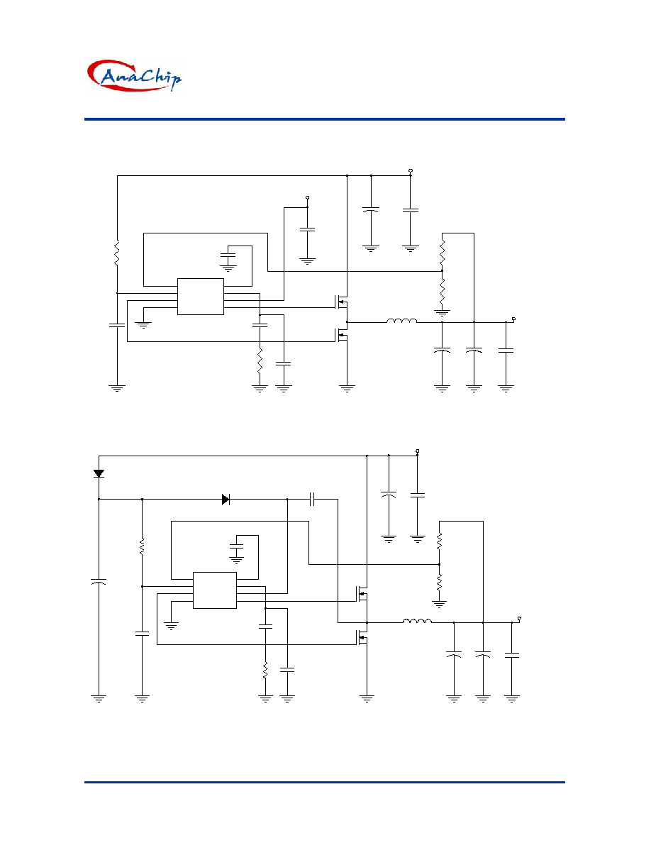
Typical Application Circuit
(1)
C6
10nF
Q2
AF9410N
C17
0.1u
VIN=5V
C3
1u
C12
470u
Vc=12V
C8
470u
Vout +1.5V/7.0A
Q1
AF9410N
L1
5.6u/9.0
R6
22k
AP2014
C13
470u
C20
100p
C5
0.47u
R3
8.2
C4
0.1u
R2
3.3K
C11
0.1u
R1
820
U1
1
2
3
4
5
6
7
8
FB
Vcc
LDrv
GND HDrv
Vc
Comp
SS
(2)
Vout +1.5V/7.0A
C5
0.47u
R3
8.2
C13
470u
C1
0.1uF
C8
470u
D1
1N4148
R2
3.3K
C11
0.1u
U1
AP2014
1
2
3
4
5
6
7
8
FB
Vcc
LDrv
GND HDrv
Vc
Comp
SS
C12
470u
R1
820
Q1
AF9410N
R6
6.8k
VIN=12V
C20
100p
Option
C4
0.1u
C6
10nF
Q2
AF9410N
C17
0.1u
1N4148
D2
C3
100u
L1
5.6u/9A
Single Supply 12V Input

AP2014/A
Synchronous PWM Controller
Anachip Corp
www.anachip.com.tw Rev. 1.2 Nov 29, 2005
5/12
Typical Application Circuit (Continued)
(3)
Vout +5V/5.0A
C5
0.47u
R3
8.2
C13
470u
C1
0.1uF
C8
470u
D1
1N4148
R2
3K
C11
0.1u
U1
AP2014
1
2
3
4
5
6
7
8
FB
Vcc
LDrv
GND HDrv
Vc
Comp
SS
R1
10K
Q1
AF4910N-1
R6
39k
VIN=12V
C20
100p
C4
0.1u
C6
10nF
Q2
AF4910N-2
C17
0.1u
1N4148
D2
C3
100u
L1
10uH/6A
Single Supply 12V Input
(4)
Vout +5V/4.0A
C5
0.47u
R3
8.2
C13
470u
C1
0.1uF
C8
470u
D1
1N4148
R2
3.3K
C11
0.1u
U1
AP2014
1
2
3
4
5
6
7
8
FB
Vcc
LDrv
GND HDrv
Vc
Comp
SS
R1
10K
Q1-1
AF4928N-1
R6
47k
VIN=24V
C20
100p
C4
0.1u
C6
10nF
Q1-2
AF4928N-2
C17
0.1u
1N4148
D2
C3
100u
L1
10uH/6A
1.2K
RZD
R3
8.2
ZD
6.2V
I
ZD
(
15mA)=(VIN-V
D2
-V
ZD
)/RZD
Single Supply 24V Input