
Universal DC/DC Converter
AP34063
This datasheet contains new product information. Anachip Corp. reserves the rights to modify the product specification without notice. No liability is assumed as a result of the use of
this product. No rights under any patent accompany the sale of the product.
Rev.A5 Feb.10, 2004
1/10
Features
∑
Operation from 3.0V to 40V Input
∑
Low Standby Current
∑
Current Limiting
∑
Output Switch Current to 1.6A
∑
Output Voltage Adjustable
∑
Frequency Operation to 100 kHz
∑
Precision 2% Reference
General Description
The AP34063 Series is a monolithic control circuit
containing the primary functions required for
DC-to-DC converters. These devices consist of an
internal temperature compensated reference,
comparator, controlled duty cycle oscillator with an
active current limit circuit, driver and high current
output switch. This series is specifically designed
for incorporating in Step-Down and Step-Up and
Voltage-Inverting applications with a minimum
number of external components.
Pin Connections
1
2
3
4
8
7
6
5
V
CC
Comparator
Inverting
Input
Driver
Collector
I
pk
Sense
Switch
Collector
Switch
Emitter
Timing
Capacitor
Gnd
(Top View)
Ordering Information
AP34063 X X X X
Package
Packing
Temp. grade
S8 : SOP-8L
N8 : PDIP-8L
Blank : Tube
A : Taping
Blank: 0
o
C~70
o
C
Lead Free
Blank : Normal
L : Lead Free Package
Universal DC/DC Converter
AP34063
Anachip Corp.
www.anachip.com.tw
Rev.A5 Feb.10, 2004
2/10
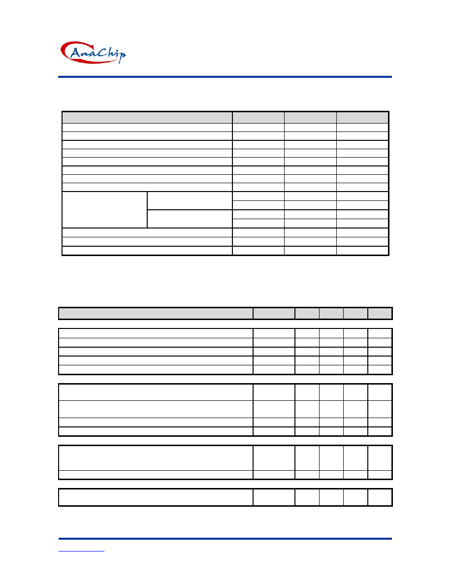
Maximum Ratings
Parameter
Symbol
Value
Unit
Power Supply Voltage
V
CC
40 V
Comparator Input Voltage Range
V
IR
-0.3
~
+40 V
Switch Collector Voltage
V
C(switch)
40
V
Switch Emitter Voltage(V
Pin
1 = 40V)
V
E(switch)
40
V
Switch Collector to Emitter Voltage
V
CE(switch)
40
V
Driver Collector Voltage
V
C(driver)
40
V
Driver Collector Current (Note 1)
I
C(driver)
100 mA
Switch Current
I
SW
1.6 A
PDIP: T
A
= 25
∞C
P
D
1.25 W
Thermal Resistance
JA
100
∞C/W
SOP: T
A
= 25
∞C
P
D
600 mW
Power Dissipation and
Thermal Characteristics
Thermal Resistance
R
JA
160
∞C/W
Operating Junction Temperature
T
J
+150
∞C
Operating Ambient Temperature Range
T
A
0
~
+70
∞C
Storage Temperature Range
T
stg
-65
~
+150
∞C
Notes: 1.Maximum package power dissipation limits must be observed.
2.ESD data available upon request.
Electrical Characteristics
(V
CC
= 5.0V, unless otherwise specified.)
Characteristics
Symbol
Min
Typ
Max
Unit
OSCILLATOR
Frequency(V
Pin
5 =0V, C
T
=1.0nF, T
A
=25
∞C)
f
osc
24 33 42 kHz
Charge Current(V
CC
=5.0V to 40V, T
A
=25
∞C)
I
chg
24 30 42 µA
Discharge Current(V
CC
=5.0V to 40V, T
A
=25
∞C)
I
dischg
140
200
260
µA
Discharge to Charge Current Ratio(Pin 7 to V
CC
, T
A
=25
∞C)
I
dischg
/ I
chg
5.2 6.5 7.5 -
Current Limit Sense Voltage(I
chg
= I
dischg
, T
A
=25
∞C)
V
ipk(sense)
300 400 450 mV
OUTPUT SWITCH (Note 3)
Saturation Voltage, Darlington Connection
(I
SW
=1.0A, Pins 1,8 connected)
V
CE(sat)
- 1.0
1.3
V
Saturation Voltage, Darlington Connection
(I
SW
=1.0A, ID = 50mA, Forced þ 20)
V
CE(sat)
-
0.45
0.7
V
DC Current Gain(I
SW
=1.0A, V
CE
=5.0V, T
A
=25
∞C)
h
FE
50
75
- -
Collector Off-State Current (V
CE
=40V)
I
C(off)
-
0.01
100
µA
COMPARATOR
Threshold Voltage
T
A
= 25
∞C
T = 0
o
C ~ 75
o
C
V
th
1.
225
1.21
1.
25
-
1.275
1.29
V
Threshold Voltage Line Regulation(V
CC
=3.0V to 40V)
Reg
line
- 1.4
6.0
mV
TOTAL DEVICE
Supply Current(V
CC
=5.0V to 40V, C
T
=1.0nF, Pin 7 = V
CC
,
V
Pin 5
> V
th
Pin 2 = Gnd, remaining pins open)
I
CC
-
-
3.5
mA

Universal DC/DC Converter
AP34063
Anachip Corp.
www.anachip.com.tw
Rev.A5 Feb.10, 2004
3/10
Note:
3.Low duty cycle pulse techniques are used during test to maintain junction temperature as close to ambient temperature as
possible.
4.If the output switch is driven into hard saturation (non-Darlington configuration) at low switch currents (
300mA) and high
driver currents (
30mA), it may take up to 2.0 µs for it to come out of saturation.? This condition will shorten the off time at
frequencies
30kHz, and is magnified at high temperatures. This condition does not occur with a Darlington configuration,
since the output switch cannot saturate. If a non-Darlington configuration is used, the following output drive condition is
recommended:
I
C
output
Forced
þ of output switch :
I
C
driver - 7.0mA*
10
*The 100 resistor in the emitter of the driver device requires about 7.0mA before the output switch conducts.
Representative Schematic Diagram
1.25V
Reference
Regulator
Ipk
Oscillator
CT
R
S Q
Q2
Q1
100
Comparator
+
_
(Bottom View)
8
7
6
5
1
2
3
4
Gnd
Timing
Capacitor
Switch
Emitter
Switch
Collector
Drive
Collector
I
pk
Sense
V
CC
Comparator
Inverting
Input

Universal DC/DC Converter
AP34063
Anachip Corp.
www.anachip.com.tw
Rev.A5 Feb.10, 2004
4/10
Figure 1. Vce(sat) versus le
0.6
0.8
1
1.2
1.4
0
0.2
0.4
0.6
0.8
1
1.2
1.4
1.6
Ie, Emitter Current (A)
Vce(sat), Saturation Voltage (V)
1.24
1.245
1.25
1.255
1.26
0
10
20
30
40
50
60
70
80
90
100
Temperature (
o
C)
Reference Voltage (V)
Figure 2. Reference Voltage versus Temp.
Figure 4. Standby Supply Current
versus Supply Voltage
0.0
0.5
1.0
1.5
2.0
2.5
3.0
3.5
4.0
0
5
10
15
20
25
30
35
40
Vcc, Supply Voltage (V)
Icc, Supply Current (
mA)
1.4
1.45
1.5
1.55
1.6
1.65
1.7
1.75
1.8
100
300
500
700
900
1100
1300
1500
I
E
(mA)
V
CE
(
sat), (V)
Figure 5. Emitter Follower Configuration
Output Saturation Voltage vs. Emitter Current
0.1
1
10
100
1000
0.01
0.1
1
10
C
T
, Oscillator Timing Capacitor (nF)
t
on-off
, Output Switch On-Off Time(us)
Figure 6.Output Switch On-Off Time versus
Oscillator Timing Capacitor
V
CC
= 5.0V
Pin 7 = V
CC
Pin 5 = GND
T
A
= 25
o
C
t
on
t
off
Vcc=2~10V
Pin1,7,8=Vcc
Pin3,5=GND
T
A
=25
o
C
Pin2=5
10W
Figure 3. Current Limit Sense Voltage
versus Temperature
320
340
360
380
400
420
440
0
10
20
30
40
50
60
70
80
90
100
Temperature (
o
C)
Current Sense Voltage (mV)

Universal DC/DC Converter
AP34063
Anachip Corp.
www.anachip.com.tw
Rev.A5 Feb.10, 2004
5/10
Application Circuit
(1) Step-Up Converter
1.25V
Ref
Reg
I
pk
C
T
R
S Q
Q2
Q1
Comp.
+
_
8
7
6
5
1
2
3
4
V
CC
Osc
180
+
470
uF
V
in
12V
R
sc
0.24
R1
10k 56k
R2
+
C
O
28V/200mA
V
out
+
100
V
out
Optional Filter
L
120uH
C
T
680
pF
1N5819
470uF
1.0uH
Test
Conditions
Results
Line Regulation
V
in
=9V to 12V, I
O
=200mA
20mV = ± 0.035%
Load Regulation
V
in
=12V, I
O
=50mA to 200mA
15mV = ± 0.035%
Output Ripple
V
in
=12V, I
O
=200mA
500mV
PP
Efficiency V
in
=12V, I
O
=200mA
80%