 | –≠–ª–µ–∫—Ç—Ä–æ–Ω–Ω—ã–π –∫–æ–º–ø–æ–Ω–µ–Ω—Ç: AP431YL | –°–∫–∞—á–∞—Ç—å:  PDF PDF  ZIP ZIP |
Adjustable Precision Shunt Regulator
AP431/AP431A
This datasheet contains new product information. Anachip Corp. reserves the rights to modify the product specification without notice. No liability is assumed as a result of the use of
this product. No rights under any patent accompany the sale of the product.
Rev.1.0 May.7, 2004
1/17
Features
∑
Precision reference voltage
AP431 : 2.495V ± 1%
AP431A : 2.495V ± 0.5%
∑
Sink current capability: 200mA
∑
Minimum cathode current for regulation: 300A
∑
Equivalent full-range temp coefficient: 30 ppm/
o
C
∑
Fast turn-on response
∑
Low dynamic output impedance: 0.2
∑
Programmable output voltage to 36v
∑
Low output noise.
∑
Packages: TO92, SOT89, SOT23, SOT25 and
SOP
Description
The AP431/AP431A are 3-terminal adjustable
precision shunt regulators with guaranteed
temperature stability over the applicable extended
commercial temperature range. The output voltage
may be set at any level greater than 2.495V(V
REF
)
up to 36V merely by selecting two external resistors
that act as a voltage divider network. These devices
have a typical output impedance of 0.2. Active
output circuitry provides very sharp turn-on
characteristics, making these devices excellent
improved replacements for Zener diodes in many
applications.
The precise (+/-) 1% Reference voltage tolerance of
the AP431/431A make it possible in many
applications to avoid the use of a variable resistor,
consequently saving cost and eliminating drift and
reliability problems associated with it.
Ordering Information
A P 4 3 1 X X X X X
Package
Packing
Blank : Tube or bulk
A : Taping
Reference Voltage
Tolerance:
Blank : +/- 1%
A : +/- 0.5%
Operating Temp. Range
Blank : SOP-8L
Y : SOT89-3L
V : TO92-3L
W : SOT23-3L
R : SOT23-3L
Q : SOT25
Blank : -20
o
C~85
o
C
I : -40
o
C~85
o
C
Lead Free
Blank : Normal
L : Lead Free Package
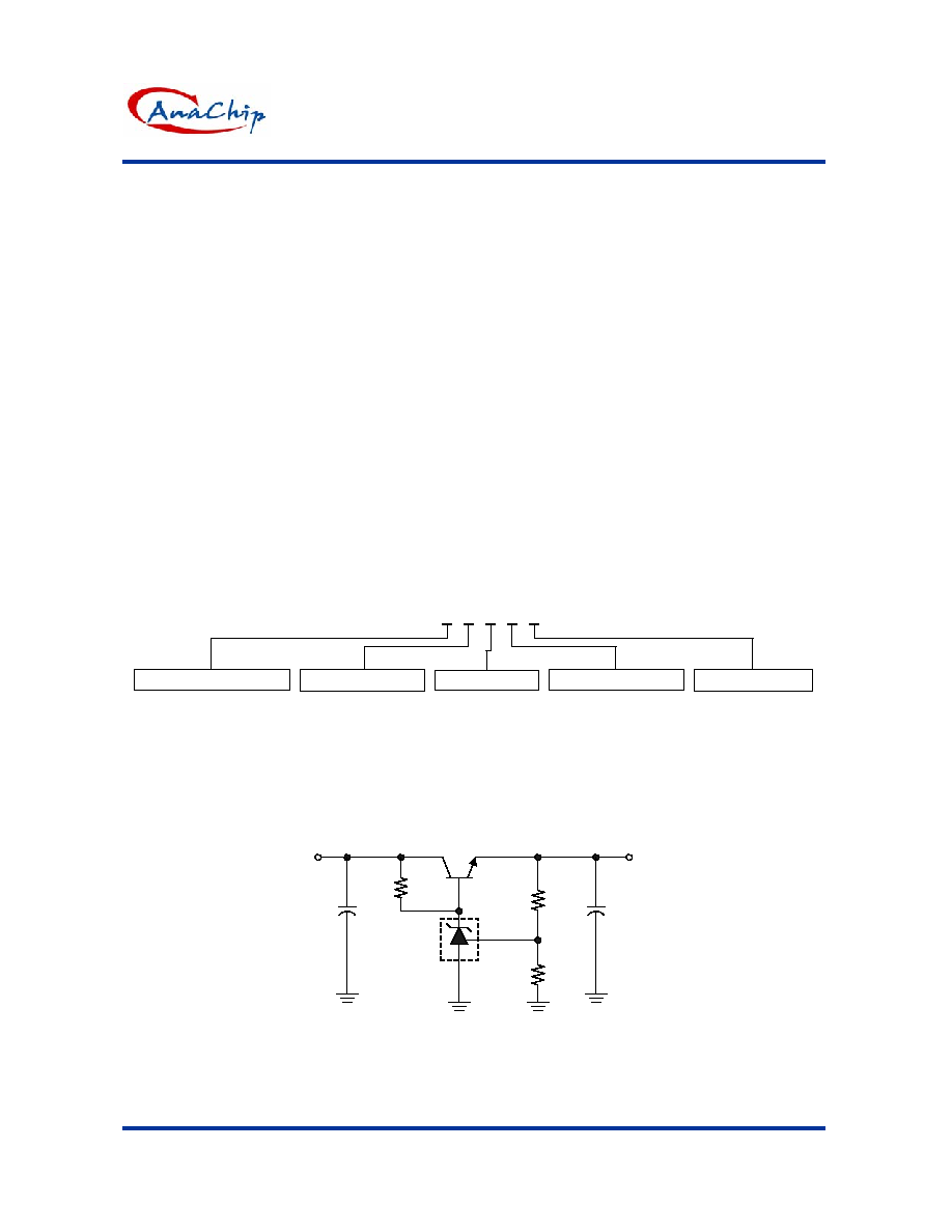
Typical Application Circuit
+
+
R2
R1
V
OUT
V
IN
V
OUT
= (1+R1/R2)V
REF
Precision Regulator
C
in
C
out
AP431
Adjustable Precision Shunt Regulator
AP431/AP431A
Anachip Corp.
www.anachip.com.tw
Rev.1.0 May.7, 2004
2/17
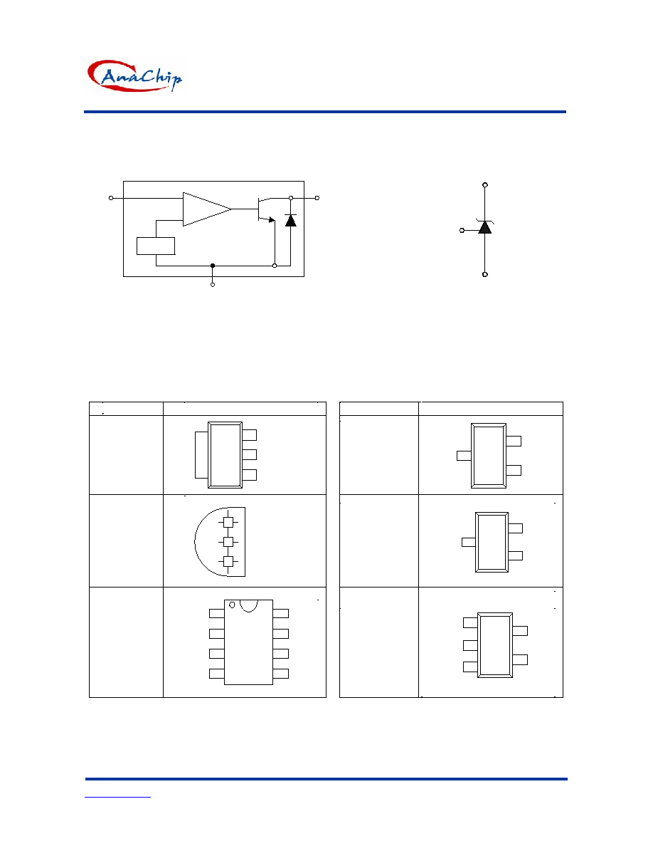
Block Diagram
REF (R)
V
REF
+
-
Anode (A)
Cat
hode (
C
)
Symbol
Cathode (C)
REF (R)
Anode (A)
Pin Configuration
Order Number
Pin Configuration (Top View)
AP431Y
AP431 AY
AP431IY
AP431IAY
(SOT89)
AP431V
AP431 AV
AP431IV
AP431IAV
(TO92)
Order Number
AP431R
AP431AR
AP431IR
AP431IAR
(SOT23)
AP431W
AP431AW
AP431IW
AP431IAW
(SOT23)
1 REF
2 Anode
3 Cathode
1 REF
2 Anode
+
+
+
3 Cathode
Anode 1
2 Cathode
3 REF
Anode 1
2 REF
3 Cathode
Cathode 1
Anode 2
Anode 3
NC 4
5 NC
6 Anode
7 Anode
8 REF
AP431
AP431A
AP431I
AP431IA
(SOP)
Pin Configuration (Top View)
AP431 Q
AP431 AQ
AP431IQ
AP431IAQ
(SOT25)
NC 1
4 REF
NC 2
Cathode 3
5 Anode
Adjustable Precision Shunt Regulator
AP431/AP431A
Anachip Corp.
www.anachip.com.tw
Rev.1.0 May.7, 2004
3/17
Marking Information
(1) SOT23 / SOT25 / SOT89
P/N Type
X X
AP431Y A
4
AP431AY A
5
AP431IY A
A
AP431IAY A
B
AP431W A
6
AP431AW A
7
AP431IW A
C
AP431IAW A
D
AP431R A
8
AP431AR A
9
AP431IR A
E
AP431IAR A
F
AP431Q A
2
AP431AQ A
3
AP431IQ A
G
AP431IAQ A
H
XX YM X
SOT23/SOT25
XX
YMX
SOT89
Date code
Y : Year
M : Month(A~L)
XX: P/N Type
(Top View)
X: Blank : normal
L : Lead Free Package
(2) SOP
Accuracy
AC
AP431X X
YYWW X
Blank:
A :
Logo
( Top view )
%
1
495
.
2
±
%
5
.
0
495
.
2
±
Blank: -20
o
C ~ +85
o
C
I : -40
o
C ~ +85
o
C
YY : Year
WW: Nth week
Date code
Temp. grade
Lead Free
Blank: normal
L: Lead Free Package
(3)TO92
Accuracy
AP431X
X YWW X X
Blank:
A :
( Top view )
Y : Year
WW: Nth week
Date code
Internal code
Temp. grade
1%
2.495
±
0.5%
2.495
±
Blank: -20
o
C ~ +85
o
C
I : -40
o
C ~ +85
o
C
Blank: normal
L: Lead Free Package
Lead Free

Adjustable Precision Shunt Regulator
AP431/AP431A
Anachip Corp.
www.anachip.com.tw
Rev.1.0 May.7, 2004
4/17
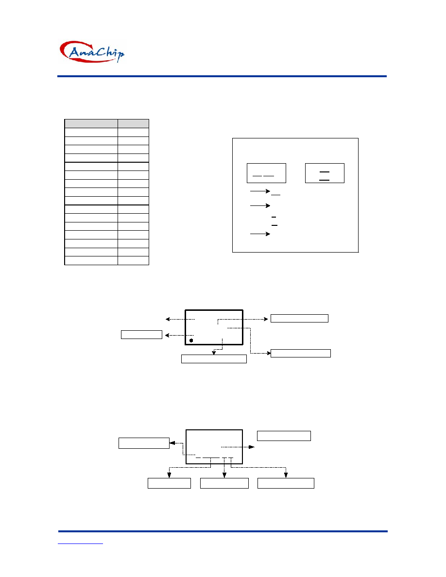
Absolute Maximum Ratings
Cathode Voltage .........................................................................................................................36V
Continuous Cathode Current ....................................................................................... -10mA ~ 250mA
Reference Input Current Range ................................................................................................... 10mA
Operating Temperature Range (AP431)............................................................................-20
o
C ~ 85
o
C
(AP431I).......................................................................... -40
o
C ~ 85
o
C
Lead Temperature................................................................................................................... 260
o
C
Storage Temperature .................................................................................................... -65
o
C ~ 150
o
C
Power Dissipation (Notes 1. 2) SOT89 Package .................................................................. 0. 80W
TO92 Package .................................................................. 0.78W
SOT23 package .................................................................. 0.25W
SOT25 Package...................................................................0.25W
SOP Package................................................................... 0.6W
Note 1: TJ, max =150
o
C
Note 2: Ratings apply to ambient temperature at 25
o
C
Electrical Characteristics
(Ta=25
o
C , unless otherwise specified.)
PARAMETER
TEST CONDITIONS
SYMBOL MIN. TYP. MAX. UNIT
AP431 2.470
2.495
2.520
Reference voltage
V
KA
= V
REF
,
I
KA
= 10mA
(Fig.1)
AP431A
V
REF
2.482 2.507
V
Deviation of Reference input voltage
over temperature (Note 3)
V
KA
= V
REF
, I
KA
= 10mA,
Ta = Full range (Fig.1)
V
REF
8.0
20
mV
V
KA
= 10V
~V
REF
V
REF
-1.4
-2.0 mV/V
Ratio of the change in Reference
voltage to the change in Cathode
voltage
I
KA
= 10mA
(Fig.2)
V
KA
= 36V ~10V
V
KA
-1 -2
mV/V
Reference input current
R1 = 10K,R2 = I
KA
= 10mA
(Fig.2)
I
REF
1.4
3.5
µA
Deviation of Reference input current
over temperature
R1 = 10K,R2 = I
KA
= 10mA
Ta = Full range (Fig.2)
I
REF
0.4
1.2
µA
Minimum Cathode current for
regulation
V
KA
= V
REF
(Fig.1) I
KA(MIN)
0.19
0.5
mA
Off-state current
V
KA
= 36V, V
REF
= 0V (Fig.3)
I
KA(OFF)
0.1
1.0
µA
Dynamic output impedance (Note 4)
V
KA
= V
REF
V
KA
= V
REF
I
KA
= 0.1mA ~ 15mA
Frequency
1KHz (Fig.1)
KA
Z
0.2
0.5
V
MAX
V
MIN
T
I
T
2
TEMPERATURE
V
DEV
= V
MAX
- V
MIN

Adjustable Precision Shunt Regulator
AP431/AP431A
Anachip Corp.
www.anachip.com.tw
Rev.1.0 May.7, 2004
5/17
Note 3. Deviation of reference input voltage, V
DEV
, is defined as the maximum variation of the reference over
the full temperature range.
The average temperature coefficient of the reference input voltage V
REF
is defined as:
1
2
6
REF
DEV
REF
T
T
10
)
C)
(25
V
V
(
V
-
∞
=
.............................................. (
)
C
ppm
∞
Where:
T2 ≠ T1 = full temperature change.
V
REF
can be positive or negative depending on whether the slope is positive or negative.
Note 4. The dynamic output impedance, R
Z
, is defined as:
KA
KA
KA
I
V
Z
=
When the device is programmed with two external resistors R1 and R2 (see Figure 2.), the dynamic output
impedance of the overall circuit, is defined as:
)
R2
R1
(1
Z
i
v
Z
KA
'
KA
+
=
Test Circuits
Input
V
REF
V
KA
I
KA
Fig1. Test Circuit for V
KA
= V
REF
IN
V
REF
R1
R2
I
REF
Note:V
KA
=V
REF
(1+R1/R2)+I
REF◊
R1
I
KA
V
KA
Fig2. Test circuit for V
KA
V
REF
IN
V
KA
I
Z(OFF)
Fig3. Test Circuit for off-state Current
Adjustable Precision Shunt Regulator
AP431/AP431A
Anachip Corp.
www.anachip.com.tw
Rev.1.0 May.7, 2004
6/17
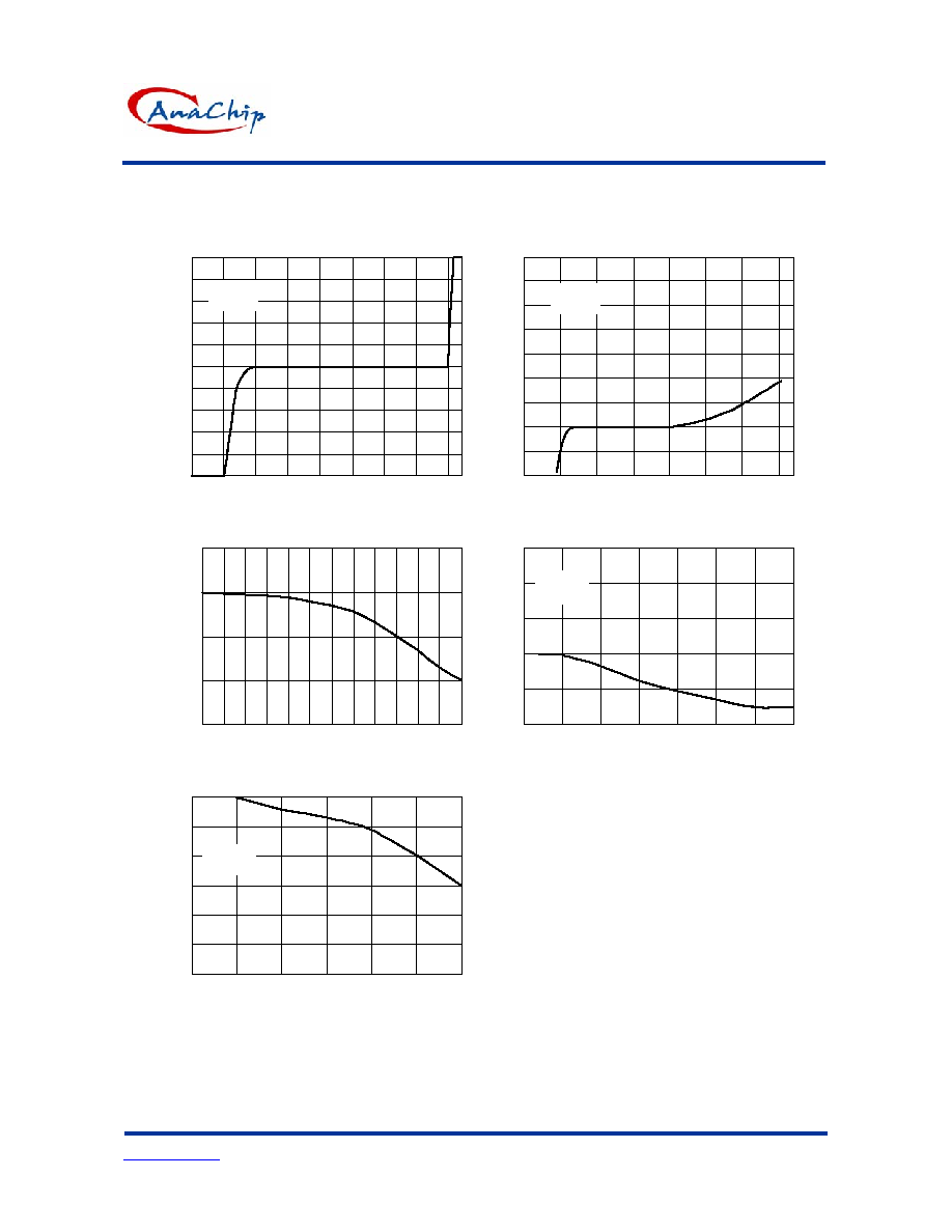
Typical Performance Characteristics
Cathode current Vs Cathode Voltage
-100
0
100
-1.5
-0.5
0.5
1.5
2.5
Cathode Voltage(v)
C
a
t
h
ode c
u
rr
ent(mA
)
V
KA
=Vref
Ta=25
o
C
Cathode current (uA) Vs Cathode Voltage
-1
Cathode Voltage(v)
Ca
t
hod
e c
u
r
r
e
n
t
(
uA
)
-200
200
400
600
0
-0.5
0
0.5
1
1.5
2
2.5
V
KA
=Vref
Ta=25
o
C
Reference Voltage Vs Free-Air Temperature
Free-Air Tempeture (
o
C)
Re
f
e
r
enc
e Volt
age
(mV
)
2480
2485
2490
2495
2500
-40
80
-30 -20 -10 0 10 20 30 40 50 60 70
Reference input current Vs free Temperature
Free-Air Temperature(
o
C)
R
e
f
e
r
enc
e
input
c
u
rr
ent (u
A
)
1
1.2
1.4
1.6
1.8
2
-50
-25
0
25
50
75
100
125
R1=10K
I
KA
=10mA
Change in Reference Voltage vs Cathode Voltage
0
5
10
15
20
25
30
Cathode Voltage (V)
C
han
ge in
Refere
nc
e V
o
l
t
age
(mv
)
-12
-10
-8
-6
-4
-2
0
I
KA
=10mA
Ta=25
o
C

Adjustable Precision Shunt Regulator
AP431/AP431A
Anachip Corp.
www.anachip.com.tw
Rev.1.0 May.7, 2004
7/17
Typical Performance Characteristics(Continued)
+
-
+
-
Output
GND
15K
8.25K
9µF
I
KA
232
TEST CIRCUIT FOR VOLTAGE AMPLIFICATION
SMALL-SIGNAL VOLTAGE AMPLIFICATION vs. FREQUENCY
0
10
20
30
40
50
60
1K
10K
100K
1M
10M
f-Frequency-Hz
A
V
-Smal
l
Si
gnal
Vol
t
age Ampl
i
f
i
c
at
i
on (dB)
I
KA
=10mA
T
A
=25
o
C
+
-
I KA
GND
Output
1K
50
TEST CIRCUIT FOR REFERENCE IMPEDANCE
REFERENCE IMPEDANCE vs. FREQUENCY
0.1
1
10
100
1K
10K
100K
1M
10M
f-Frequency-Hz
ZK
A
--
Reference Impedance
--
I
KA
=10mA
T
A
=25
o
C
Adjustable Precision Shunt Regulator
AP431/AP431A
Anachip Corp.
www.anachip.com.tw
Rev.1.0 May.7, 2004
8/17
PULSE RESPONSE
0
1
2
3
4
5
6
-1
0
1
2
3
4
5
6
7
t-Time-µ S
Input and Output Voltage-V
Input
Output
GND
Output
220
50
TEST CIRCUIT FOR PULSE RESPONSE
Pulse
Generator
f=100kHz
T
A
=25
o
C
+
-
150
I KA
V
BATT
C
L
TEST CIRCUIT FOR CURVE A
+
-
C
L
R1=10K
R2
I KA
150
V
BATT
TEST CIRCUIT FOR CURVE B, C, AND D
The areas under the curves represent conditions that may cause the
device to oscillate. For curves B, C, and D, R2 and V+ were adjusted
to establish the initial V
KA
and I
KA
conditions with C
L
=0.V
BATT
and
C
L
were then adjusted to determine the ranges of stability.
STABILITY BOUNDARY CONDITIONS
0
10
20
30
40
50
60
70
80
90
100
0.001
0.01
0.1
1
10
C
L
-Load Capacitance-µF
I
KA
-Cathode Current-m
A
A V
KA
=V
ref
B V
KA
=5V
C V
KA
=10V
D V
KA
=15V
A
B
C
D
Stable
Stable
TA=25
o
C
Adjustable Precision Shunt Regulator
AP431/AP431A
Anachip Corp.
www.anachip.com.tw
Rev.1.0 May.7, 2004
9/17
Application Examples
V
IN
+
Low Limit V
REF
(1 + R1B/R2B) +V
BE
High Limit V
REF
(1 + R1A/R2A)
R1A
R1B
R2A
R2B
V
BE
Output ON when
Low Limint < V
IN
< High Limit
Fig.10 Over-Voltage / Under-Voltage Protection Circuit
V
IN
R
CL
I
OUT
I
OUT
= V
REF
/ R
CL
Fig.6 Current Limiter or Current Source
I
OUT
V
IN
I
OUT
= V
REF
/ R
S
R
S
Fig.7 Constant-Current Sink
Fig.4 Voltage Monitor
Fig.5 Delay Timer
V
OUT
= (1 + R1/R2) x V
REF
V
IN
R1
R2
Fig.8 Higher-Current Shunt Regulator
V
OUT
V
IN
PUSE
R1
R2
L
IMIT
(1 + R1/R2) x V
REF
Fig.9 Crow Bar
V
OUT
V
IN
ON
OFF
R
+
V
IN
Delay = RC x ln(
V
IN
-V
REF
)
LED on when Low LimitV
IN
High Limit
Low Limit V
REF
(1+R1B/R2B)
High Limit V
REF
(1+R1A/R2A)
R1A
R2A
V
IN
R1B
R2B

Adjustable Precision Shunt Regulator
AP431/AP431A
Anachip Corp.
www.anachip.com.tw
Rev.1.0 May.7, 2004
10/17
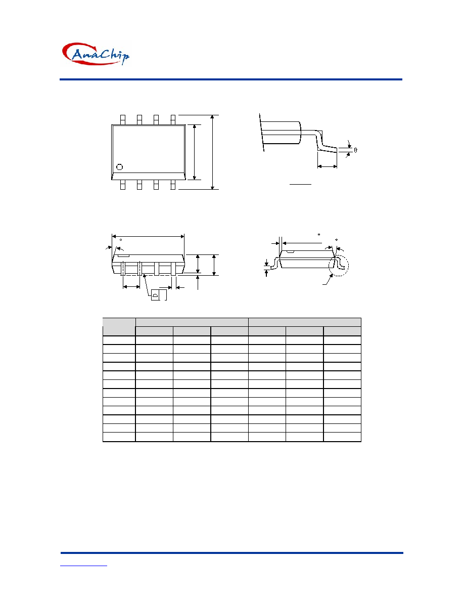
Package Diagrams
(1) SOT89-3L Package Outline Dimension
c
5
0
(2x)
L
HE
E
D1
e1
e
A
D
b1
b
b
8
0
(2x)
Dimensions In Millimeters
Dimensions In Inches
Symbol
Min.
Nom.
Max.
Min.
Nom.
Max.
A 1.40
1.50
1.60
0.055
0.059
0.063
b 0.36
0.42
0.48
0.014
0.016
0.018
b1 0.41
0.47
0.53
0.016
0.043
0.051
C 0.35
0.39
0.43
0.014
0.015
0.017
D 4.40
4.50
4.60
0.173
0.177
0.181
D1 1.40
1.60
1.75
0.055
0.062
0.069
e 2.90
3.00
3.10
0.114
0.118
0.122
e1 1.45
1.50
1.55
0.057
0.059
0.061
E 2.40
2.50
2.60
0.094
0.098
0.102
HE 3.94 - 4.25
0.155 - 0.167
L 0.80 - 1.20
0.031 -
0.047

Adjustable Precision Shunt Regulator
AP431/AP431A
Anachip Corp.
www.anachip.com.tw
Rev.1.0 May.7, 2004
11/17
(2) TO92-3L Package Outline Dimension
D
b
b
1
b
E
L
e
A
1
A
Dimensions In Millimeters
Dimensions In Inches
Symbol
Min.
Nom.
Max.
Min.
Nom.
Max.
A 3.302 3.556 3.810 0.130 0.140 0.150
A1
1.016 - - 0.040 - -
b 0.330 0.381 0.432 0.013 0.015 0.017
b1 0.406 0.457 0.506 0.016 0.018 0.020
D 4.445 4.572 4.699 0.175 0.180 0.185
E 4.445 4.572 4.699 0.175 0.180 0.185
L 13.00 - 15.500
0.512 - 0.610
e 1.150 1.270 1.390 0.045 0.050 0.055
Adjustable Precision Shunt Regulator
AP431/AP431A
Anachip Corp.
www.anachip.com.tw
Rev.1.0 May.7, 2004
12/17
(3) SOT23-5L Package Outline Dimension
Gauge Plane
0.25 mm
L
L1
E1
E
e1
D
1
2
3
4
5
b
e
b1
b
C
C1
Base
Metal
With
Plating
A2
A1
A
Seating Plane
0.10 C
5x
2(4x)
1(4x)
Dimensions In Millimeters
Dimensions In Inches
Symbol
Min.
Nom.
Max.
Min.
Nom.
Max.
A
1.05 1.20 1.35 0.041 0.047 0.053
A1 0.05 0.10 0.15 0.002 0.004 0.006
A2 1.00 1.10 1.20 0.039 0.043 0.047
b 0.25 - 0.55
0.010
-
0.022
b1 0.25 0.40 0.45 0.010 0.016 0.018
c 0.08 - 0.20
0.003
-
0.008
c1 0.08
0.11
0.15
0.003
0.004
0.006
D
2.70 2.85 3.00 0.106 0.112 0.118
E
2.60 2.80 3.00 0.102 0.110 0.118
E1 1.50 1.60 1.70 0.059 0.063 0.067
L
0.35 0.45 0.55 0.014 0.018 0.022
L1 0.60
Ref.
0.024
Ref.
e 0.95
Bsc.
0.037
Bsc.
e1 1.90
Bsc.
0.075
Bsc.
0
o
5
o
10
o
0
o
5
o
10
o
1
3
o
5
o
7
o
3
o
5
o
7
o
2
6
o
8
o
10
o
6
o
8
o
10
o
Adjustable Precision Shunt Regulator
AP431/AP431A
Anachip Corp.
www.anachip.com.tw
Rev.1.0 May.7, 2004
13/17
(4) SOT23-3L Package Outline Dimension
C
L
e
E
HE
2
1
3
D
A2
A1
b
A
Dimensions In Millimeters
Dimensions In Inches
Symbol
Min.
Nom.
Max.
Min.
Nom.
Max.
A
1.00 1.20 1.40 0.039
0.047 0.055
A1 0.00 - 0.10
0.000 - 0.004
A2 1.00 1.15 1.30 0.039
0.045 0.051
b 0.35 - 0.50
0.014
-
0.020
C
0.10 0.175 0.25 0.004 0.007 0.010
D
2.70 2.90 3.10 0.106
0.114 0.122
E
1.40 1.60 1.80 0.055
0.063 0.071
e
1.70 2.00 2.30 0.067
0.079 0.091
HE 2.40 2.70 3.00 0.094
0.106 0.118
L 0.30 - 0.55
0.012
-
0.022
Adjustable Precision Shunt Regulator
AP431/AP431A
Anachip Corp.
www.anachip.com.tw
Rev.1.0 May.7, 2004
14/17
(5) SOP-8L Package Outline Dimension
VIEW "A"
L
C
VIEW "A"
H
E
A
A2
A1
B
e
D
7 (4X)
0.015x45
7 (4X)
y
Dimensions In Millimeters
Dimensions In Inches
Symbol
Min.
Nom.
Max.
Min.
Nom.
Max.
A 1.40 1.60 1.75
0.055
0.063
0.069
A1 0.10 - 0.25 0.040 - 0.100
A2 1.30 1.45 1.50 0.051
0.057
0.059
B 0.33 0.41 0.51
0.013
0.016
0.020
C 0.19 0.20 0.25
0.0075
0.008
0.010
D 4.80 5.05 5.30 0.189
0.199
0.209
E 3.70 3.90 4.10
0.146
0.154
0.161
e - 1.27 - -
0.050
-
H 5.79 5.99 6.20 0.228
0.236
0.244
L 0.38 0.71 1.27
0.015
0.028
0.050
y - - 0.10 - -
0.004
0
O
- 8
O
0
O
- 8
O
Adjustable Precision Shunt Regulator
AP431/AP431A
Anachip Corp.
www.anachip.com.tw
Rev.1.0 May.7, 2004
15/17
Taping Information
(1)TO92 TAPING
Po
M
Ho
T
F2 F1
Do
A
h
Millimeters
Inches
Symbol
Min.
Typ.
Max.
Min.
Typ.
Max.
Po 12.4 12.7 13.0 0.488
0.500
0.512
M 2.0 2.5 3.0 0.079
0.098
0.118
Ho 15.5 16.0 16.5 0.610
0.630
0.650
Do - 4.0 - -
0.157 -
A - 6.0 - -
0.236 -
h
0.0 - 1.0
0.000
-
0.039
T - 18.0 - -
0.709 -
F1 2.4 2.5 2.9 0.094
0.098
0.114
F2 2.4 2.5 2.9 0.094
0.098
0.114
30 ±1mm
90 ±1mm
76 ±1mm
360 ±2mm
45mm
53 ±2mm
E
330mm
40mm
205mm
Adjustable Precision Shunt Regulator
AP431/AP431A
Anachip Corp.
www.anachip.com.tw
Rev.1.0 May.7, 2004
16/17
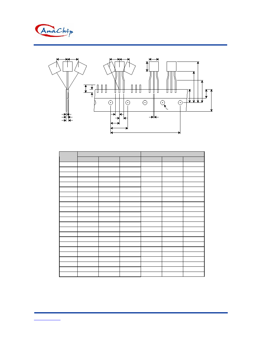
(2)TO92 TAPING
H2A
H2A
D1
F1
F2
P1
P
P2
D
L
L1
A
D2
H1
H4
H3
H
W1
W
H2
H2
T2
T
T1
Millimeters
Inches
Symbol
Min.
Typ.
Max.
Min.
Typ.
Max.
A 3.18 7.59 12 0.125 0.299 0.472
D 3.8
4
4.2 0.150 0.157 0.165
D1 0.36 0.445 0.53 0.014 0.018 0.021
D2 - - 9.0 - - 0.354
F1,F2
2.4 2.5 2.7 0.094
0.098
0.106
F1-F2 - 0.30 -
- ±0.012 -
H 15.5 16 16.5 0.610 0.630 0.650
H1 8.5
9
9.5 0.335 0.354 0.374
H2 - - 0.5 - - 0.020
H2A
- - 0.5 - - 0.020
H3 - - 27 - - 1.063
H4 - - 20 - - 0.787
L - - 11 - -
0.433
L1 2.5 - - 0.098 - -
P 12.5 12.7 12.9 0.492
0.500
0.508
P1 5.95 6.35 6.75 0.234
0.250
0.266
P2 50.3 50.8 51.3 1.980
2.000
2.020
T - - 0.55 - -
0.022
T1 - - 1.42 - - 0.056
T2 0.36 0.52 0.68 0.014
0.020
0.027
W 17.5 18.25 19 0.689
0.719
0.748
W1
5 6 7
0.197
0.236
0.276
----* 253 254 255 9.961
10.000
10.039
----* = every 20 pcs distance.
Adjustable Precision Shunt Regulator
AP431/AP431A
Anachip Corp.
www.anachip.com.tw
Rev.1.0 May.7, 2004
17/17
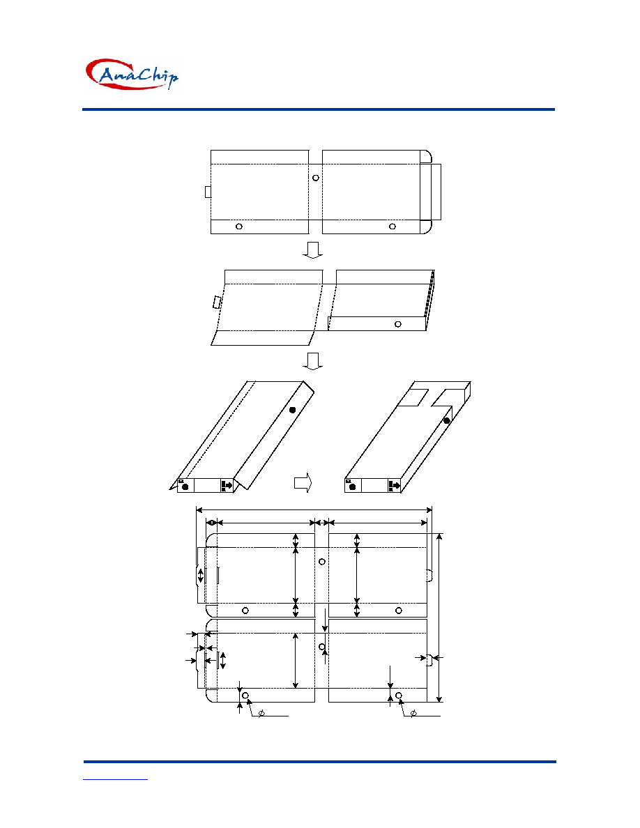
BOX Dimension
53
195
40
40
70
195
40
197
40.5
40.5
41
330
24
556
811.5
330
37.5
6
43
4.68
18.18
16.67
18.68
38.5
39.5
unit:mm.