 | –≠–ª–µ–∫—Ç—Ä–æ–Ω–Ω—ã–π –∫–æ–º–ø–æ–Ω–µ–Ω—Ç: AP432QLA | –°–∫–∞—á–∞—Ç—å:  PDF PDF  ZIP ZIP |
Adjustable Precision Shunt Regulator
AP432/AP432A
This datasheet contains new product information. Anachip Corp. reserves the rights to modify the product specification without notice. No liability is assumed as a result of the use of
this product. No rights under any patent accompany the sale of the product.
Rev.1.0 May.7, 2004
1/16
Features
- Precision reference voltage
AP432 : 1.24V ± 1%
AP432A : 1.24V ± 0.5%
- Sink current capability: 200mA.
- Minimum cathode current for regulation: 150µA
- Equivalent full-range temp coefficient: 30 ppm/
o
C
- Fast turn-on Response.
- Low dynamic output impedance: 0.2
- Programmable output voltage to 20v
- Low output noise
- Packages: SOT89, SOT23, SOT25, SOP8 and
TO92
General Description
The AP432/432A are 3-terminal adjustable
precision shunt regulators with guaranteed stable
temperature over the applicable extended
commercial temperature range. The output voltage
may be set at any level greater than 1.24\/ (V
REF
) up
to 20V merely by selecting two external resistors
that act as a voltage divider network. These devices
have a typical output impedance of 0.2. Active
output circuitry provides very sharp turn-on
characteristics, making these devices excellent
improved replacements for Zener diodes in many
applications.
The precise +/- 1% reference voltage tolerance of
the AP432/432A make it possible in many
applications to avoid the use of a variable resistor,
consequently saving cost and eliminating drift and
reliability problems associated with it.
Ordering Information
A P 4 3 2 X X X X X
Package
Packing
Blank : Tube or bulk
A : Taping
Reference Voltage
Operating Temp. Range
Blank : SOP-8L
Y : SOT89-3L
V : TO92-3L
W : SOT23-3L
R : SOT23-3L
Q : SOT25
Blank : -20
o
C~85
o
C
I : -40
o
C~85
o
C
Lead Free
Blank : Normal
L : Lead Free Package
Tolerance:
Blank : 1.24V(+/-) 1%
A : 1.24V(+/-) 0.5%
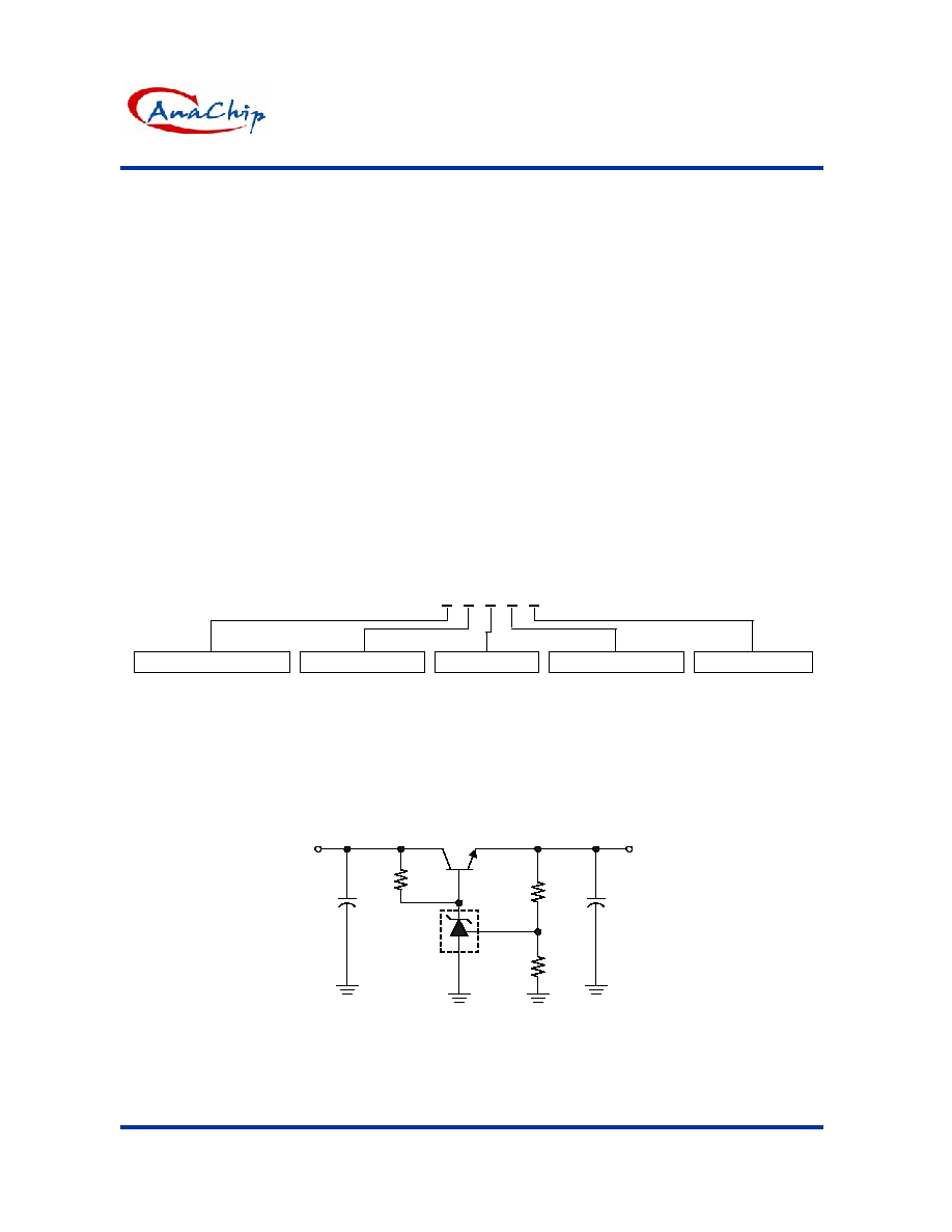
Typical Application Circuit
+
+
R2
R1
V
OUT
V
IN
V
OUT
= (1+R1/R2)V
REF
Precision Regulator
C
in
C
out
AP432

Adjustable Precision Shunt Regulator
AP432/AP432A
Anachip Corp.
www.anachip.com.tw
Rev.1.0 May.7, 2004
2/16
Block Diagram
REF (R)
V
REF
+
-
Anode (A)
Cathode (C)
1.24V
Symbol
Cathode (C)
REF (R)
Anode (A)
Pin Configuration
Order Number
Pin Configuration (Top View)
AP432Y
AP432 AY
AP432IY
AP432IAY
(SOT89)
AP432V
AP432 AV
AP432IV
AP432IAV
(TO92)
Order Number
AP432R
AP432AR
AP432IR
AP432IAR
(SOT23)
AP432W
AP432AW
AP432IW
AP432IAW
(SOT23)
1 REF
2 Anode
3 Cathode
1 REF
2 Anode
+
+
+
3 Cathode
Anode 1
2 Cathode
3 REF
Anode 1
2 REF
3 Cathode
Cathode 1
Anode 2
Anode 3
NC 4
5 NC
6 Anode
7 Anode
8 REF
AP432
AP432A
AP432I
AP432IA
(SOP)
Pin Configuration (Top View)
AP432 Q
AP432 AQ
AP432IQ
AP432IAQ
(SOT25)
NC 1
4 REF
NC 2
Cathode 3
5 Anode

Adjustable Precision Shunt Regulator
AP432/AP432A
Anachip Corp.
www.anachip.com.tw
Rev.1.0 May.7, 2004
3/16
Marking Information
(1) SOT23 / SOT25 / SOT89
P/N Type
X X
AP432Y B1
AP432AY B2
AP432IY BA
AP432IAY BB
AP432W B3
AP432AW B4
AP432IW BC
AP432IAW BD
AP432R B5
AP432AR B6
AP432IR BE
AP432IAR BF
AP432Q B7
AP432AQ B8
AP432IQ BG
AP432IAQ BH
XX YM X
SOT23/SOT25
XX
YMX
SOT89
Date code
Y : Year
M : Month(A~L)
XX: P/N Type
(Top View)
X: Blank : normal
L : Lead Free Package
(2) SOP
Accuracy
AC
AP432X X
YYWW X
Blank:
A :
Logo
( Top view )
1%
1.24
±
0.5%
1.24
±
Blank: -20
o
C ~ +85
o
C
I : -40
o
C ~ +85
o
C
YY : Year
WW: Nth week
Date code
Temp. grade
Lead Free
Blank: normal
L: Lead Free Package
(3) TO92
Accuracy
AP432X
X YWW X X
Blank:
A :
( Top view )
Y : Year
WW: Nth week
Date code
Internal code
Temp. grade
1%
1.24
±
0.5%
1.24
±
Blank: -20
o
C ~ +85
o
C
I : -40
o
C ~ +85
o
C
Blank: normal
L: Lead Free Package
Lead Free

Adjustable Precision Shunt Regulator
AP432/AP432A
Anachip Corp.
www.anachip.com.tw
Rev.1.0 May.7, 2004
4/16
Absolute Maximum Ratings
Cathode Voltage........................................................................................................20V
Continuous cathode current .....................................................................................-10mA ~ 250mA
Reference input current range ...................................................................................................10mA
Operating temperature range (AP432) ........................................................................ -20
o
C ~ 85
o
C
(AP432I............................................................................... -40
o
C~85
o
C
Lead Temperature....................................................................................................260
o
C
Storage Temperature ............................................................................................-65
o
C ~ 150
o
C
Power Dissipation (Notes 1. 2) SOT89 .................................................................... 0. 80W
TO92............................................................... ..... 0.78W
SOT23 .................................................................. 0.25W
SOT25....................................................................0.25W
SOP..................................................................... 0.6W
Note 1: TJ, max =150
o
C. .
Note 2: Ratings apply to ambient temperature at 25
o
C.
Electrical Characteristics
(Ta=25
o
C, unless otherwise specified.)
Parameter
Test conditions
Symbol Min.
Typ.
Max.
Unit
AP432 1.227
1.252
Reference voltage
V
KA
= Vref,
I
KA
= 10mA
(Fig.1)
AP432A
V
REF
1.233
1.24
1.246
V
Deviation of reference input voltage
over temperature (Note 3)
V
KA
= V
REF
, I
KA
= 10mA ,
Ta = full range (Fig.1)
V
REF
3.0 20 mV
Ratio of the change in reference
voltage to the change in cathode
voltage
I
KA
= 10mA
(Fig.2)
V
KA
= 20 ~V
REF
KA
REF
V
V
-1.4 -2.0 mV/V
Reference input current
R1 = 10K,R2 =
I
KA
= 10mA (Fig.2)
I
REF
1.4
3.5
µA
Deviation of reference input current
over temperature
R1 = 10K,R2 =
I
KA
= 10mA
Ta = Full range (Fig.2)
I
REF
0.4
1.2
µA
Minimum cathode current for
regulation
V
KA
= V
REF
(Fig.1) I
KA(min)
0.15
0.3
mA
Off-state current
V
KA
= 20V , V
REF
= 0V (Fig.3) I
KA(off)
0.1
1.0
µA
Dynamic output impedance (Note 4)
V
KA
= V
REF
I
KA
= 0.1mA ~ 15mA
Frequency
1KHz (Fig.1)
KA
Z
0.2
0.5

Adjustable Precision Shunt Regulator
AP432/AP432A
Anachip Corp.
www.anachip.com.tw
Rev.1.0 May.7, 2004
5/16
V
MAX
V
MIN
T
I
T
2
TEMPERATURE
V
DEV
= V
MAX
- V
MIN
Note 3. Deviation of reference input voltage, V
DEV
, is defined as the maximum variation of the reference over
the full temperature range.
The average temperature coefficient of the reference input voltage V
REF
is defined as:
1
2
6
C)
(25
REF
DEV
REF
T
T
10
)
V
V
(
V
-
◊
∞
=
.............................................. (
)
C
ppm
∞
Where:
T2 ≠ T1 = full temperature change.
V
REF
can be positive or negative depending on whether the slope is positive or negative.
Note 4. The dynamic output impedance, R
Z
, is defined as:
KA
KA
KA
I
V
Z
=
When the device is programmed with two external resistors R1 and R2 (see Figure 2.), the dynamic output
impedance of the overall circuit, is defined as:
)
(
R2
R1
1
Z
i
v
'
Z
KA
KA
+
=
Test Circuits
Input
V
REF
V
KA
I
KA
Fig1. Test Circuit for V
KA
= V
REF
IN
V
REF
R1
R2
I
REF
I
KA
V
KA
Fig2. Test circuit for V
KA
V
REF
IN
V
KA
I
Z(OFF)
Fig3. Test Circuit for off-state Current
R1
I
)
R2
R1
(1
V
V
REF
REF
KA
+
+
=