
Single Phase Hall Effect Latch
ATS477
This datasheet contains new product information. Anachip Corp. reserves the rights to modify the product specification without notice. No liability is assumed as a result of the use of
this product. No rights under any patent accompany the sale of the product.
Rev. A5 Apr 15, 2004
1/7
ATC
Features
- On-chip Hall sensor
- Bi-direction H type output drivers for single coil
- Internal bandgap regulator allows temperature
compensated operations and a wide operating
voltage range
- High output sinking capability up to 250mA
- Operating voltage: 3.5V~20V
- Low output switching current noise
- Build-in shunt Zener protection for output driver
- SOP-7L provide FG output pin
- Package: SIP-4L and SOP-7L
Applications
- Single-coil Brush-less DC Fan
- Single-coil Brush-less DC Motor
General Description
ATS477 that integrates Hall sensor with output
drivers is designed for electrical commutation of
brush-less DC motor application. The device
includes on-chip Hall voltage generator for
magnetic sensing, the error amplifier that amplifies
the Hall voltage, a comparator that is to provide
switching hysteresis for noise rejection, the
bi-direction drivers for sinking and driving large
current load, and the frequency generator (FG) that
provides a signal proportional to rotation speed.
Internal bandgap regulator is used to provide
temperature compensated bias for internal circuits
and allows a wide operating supply voltage range.
Built-in protection circuit and output shunt Zener
diodes were applied for protecting output drivers
during operating.
If a magnetic flux density is larger than threshold
Bop, DO is turned to sink and DOB is turned to
drive. The output state is held until a magnetic flux
density reversal falls below Brp causing DO to be
turned to drive and DOB turned to sink.
ATS477 is rated for operation over-temperature
range from -20
o
C to 85
o
C and voltage range from
3.5V to 20V. The devices are available in low cost
die forms or rugged SIP-4L and power SOP-7L
packages.
Ordering Information
ATS477 X - X X X - X
Packing
Blank : Tube or Bulk
A : Tape & Reel
P: SIP-4L
Package
Lead
L : Lead Free
Blank: Normal
Wafer Body
Magnetic
Characteristics
Blank or
A~Z : if necessary
to specify
A or B
S: SOP-7L
Application Circuit
Vcc
1
2
3
4
coil
coil
1
5
4
3
2
6
7
FG
Vcc
(SIP-4L) (SOP
7)
Single-coil brush-less DC Fan

Single Phase Hall Effect Latch
ATS477
Anachip Corp.
www.anachip.com.tw
Rev. A5 Apr 15, 2004
4/7
ATC
Absolute Maximum Ratings
( at Ta=25
o
C )
Characteristics
Symbol
Values
Unit
Supply voltage
V
CC
20 V
Magnetic flux density
B
Unlimited
Continuous 250
Hold 300
Output "on" current
Peak (Start Up)
Ic
600
mA
Operating temperature range
T
a
-20~+85
�C
Storage temperature range
T
s
-65~+150
�C
SIP-4L 550
mW
Package Power
Dissipation
SOP-7L
PD
800
mW (Note 1)
(Note 1) Ground pin must connect to large area copper on PCB as possible.
Electrical Characteristics
( Ta=+25
�C, Vcc=3.5V to 20V )
Characteristic
Symbol
Test Conditions
Min
Typ Max Unit
Supply Voltage
Vcc
3.5
20 V
Vce(sink)
Vcc=14V, Ic=200mA
500 800 mV
Output Saturation
Voltage
Vce(drive)
Vcc=14V, Ic=200mA
Vcc-1.5
Vcc V
FG Saturation Voltage
Vce
Vcc=14V, I
FG
=20mA
0.3
0.7
V
Supply Current
Icc
Vcc=20V, Output Open
18 30 mA
Output Rise Time
tr
Vcc=14V, RL=820
, CL=20pF
1.0 5.0 �s
Output Falling Time
tf
Vcc=14V, RL=820
, CL=20pF
0.3 1.5 �s
Switch Time Differential
t Vcc=14V,
RL=820
, CL=20pF
1.0 5.0 �s
Magnetic Characteristics
(Ta=+25
�C)
(1mT=10Gauss)
A grade
Characteristic
Symbol
Min.
Typ.
Max.
Unit
Operate Point
Bop
5
-
70
Gauss
Release Point
Brp
-70
-
-5
Gauss
Hysteresis Bhy
-
60
-
Gauss
B grade
Characteristic
Symbol
Min.
Typ.
Max.
Unit
Operate Point
Bop
-
-
100
Gauss
Release Point
Brp
-100
-
-
Gauss
Hysteresis Bhy
-
60
-
Gauss
Single Phase Hall Effect Latch
ATS477
Anachip Corp.
www.anachip.com.tw
Rev. A5 Apr 15, 2004
5/7
ATC
12
10
8
6
4
2
OFF
OP
RP
ON
Output Voltage in Volts
12
10
8
6
4
2
OP
ON
OFF
RP
Output Voltage in Volts
-200
200
100
-100
0
-200
200
100
-100
0
HYSTERCSIS CHARACTERISTICS
Magnetic Flux Density in Gauss
Magnetic Flux Density in Gauss
DOB
DO
Vsat
Vsat
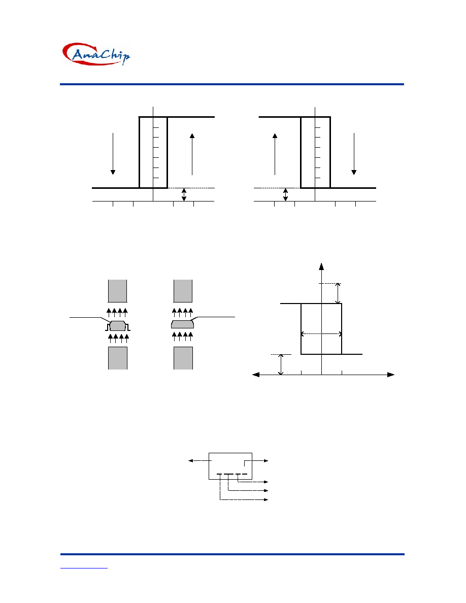
Operation Characteristics
Marking side
S
B
hy
V
sat
V
cc
( Output Voltage )
V
d
B
rp
B
op
0
( Magnetic flux density )
DO
High
Low
Marking side
S
( SIP4 )
( SOP-7 )
N
N
Marking Information
477
Part Number
Year:
( Top View )
"2" = 2002
"1" = 2001
X XX X X
Nth week: 01~52
ID Code: A ~ Z
Blank : normal
L : Lead Free Package
~

