AAT3223
250mA NanoPowerTM LDO
Linear Regulator with Power OK
3223.2004.07.1.3
1
PowerLinear
TM
General Description
The AAT3223 PowerLinearTM NanoPower Low
Dropout Linear Regulator is ideal for portable appli-
cations where extended battery life is critical. This
device features extremely low quiescent current
which is typically 1.1ĶA. Dropout voltage is also
very low, typically 190mV at 100mA. The AAT3223
has an Enable pin feature, which when pulled low
will put the LDO regulator into a shutdown mode
removing power from its load and offering extend-
ed power conservation capabilities for portable bat-
tery powered applications. The AAT3223 also has
a Power OK (POK) feature. The POK function
monitors the LDO output voltage and will alert the
system if the output falls out of regulation.
The AAT3223 has output short circuit and over cur-
rent protection. In addition, the device also has an
over temperature protection circuit, which will shut-
down the LDO regulator during extended over cur-
rent event events.
The AAT3223 is available in a space saving 6-pin
SOT23 or 8-pin SC70JW package. The device is
rated over a -40įC to 85įC temperature range.
The AAT3223 is similar to the AAT3221 with the
exception that it offers the additional Power OK
function through the POK pin.
Features
∑
1.1 ĶA Quiescent Current
∑
250 mA Output Current
∑
Low Dropout: 190 mV (typical)
∑
High accuracy: Ī2%
∑
Current limit protection
∑
Over-Temperature protection
∑
Extremely Low power shutdown mode
∑
Low Temperature Coefficient
∑
Factory programmed output voltages
∑
Stable operation with virtually any output
capacitor type
∑
Power OK signal output
∑
Active high Enable pin
∑
6-pin SOT23 or 8-pin SC70JW package
∑
4kV ESD
Applications
∑
Cellular Phones
∑
Notebook Computers
∑
Portable Communication Devices
∑
Handheld Electronics
∑
Remote Controls
∑
Digital Cameras
∑
PDAs
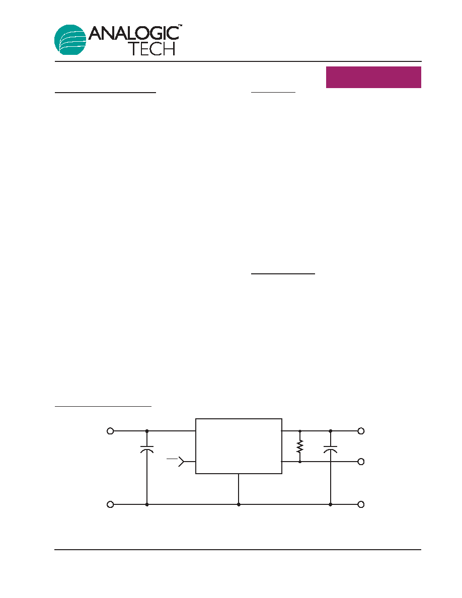
Typical Application
AAT3223
1
Ķ
F
1
Ķ
F
OUT
IN
POK
EN
GND
V
OUT
GND
GND
V
IN
ON/OFF
100k
POK
Pin Descriptions
Pin Configuration
AAT3223
AAT3223
SC70JW-8
SOT23-6
(Top View)
(Top View)
GND
POK
EN
N/C
OUT
IN
1
2
3
4
5
6
OUT
IN
POK
GND
GND
GND
GND
EN
1
2
3
4
5
6
7
8
Pin #
Symbol
Function
SOT23-6
SC70JW-8
1
3
IN
Input pin. It is recommended to bypass this pin with a 1ĶF
capacitor
2
5, 6, 7, 8
GND
Ground connection pin
3
2
OUT
Output pin. This pin should be decoupled with a 1ĶF or larg-
er capacitor.
4
N/C
Not connected
5
1
EN
Enable input. Active high, logic level compatible.
6
4
POK
Power OK output pin. This pin pulled to ground during a
power failure, it is normally high impedance and should have
a 100k
pull-up resistor connected to OUT.
AAT3223
250mA NanoPowerTM LDO
Linear Regulator with Power OK
2
3223.2004.07.1.3
Absolute Maximum Ratings
(T
A
=25įC unless otherwise noted)
Note: Stresses above those listed in Absolute Maximum Ratings may cause permanent damage to the device. Functional operation at con-
ditions other than the operating conditions specified is not implied. Only one Absolute Maximum rating should be applied at any one time.
Thermal Information
Note 1: Mounted on a demo board.
Note 2: Derate 6.7mW/įC above 25įC.
Recommended Operating Conditions
Note 3: To calculate minimum input voltage, use the following equation: V
IN(MIN)
= V
OUT(MAX)
+ V
DO(MAX)
as long as V
IN
2.5V.
Symbol
Description
Rating
Units
V
IN
Input Voltage
3
(V
OUT
+V
DO
) to 5.5
V
T
Ambient Temperature Range
-40 to +85
įC
Symbol
Description
Rating
Units
JA
Thermal Resistance (SOT23-6, SC70JW-8)
1
150
įC/W
P
D
Power Dissipation (SOT23-6, SC70JW-8) (T
A
= 25įC)
1, 2
667
mW
Symbol
Description
Value
Units
V
IN
Input Voltage
-0.3 to 6
V
V
EN
EN to GND Voltage
-0.3 to 6
V
V
ENIN(MAX)
Maximum EN to Input Voltage
0.3
V
I
OUT
Maximum DC Output Current
P
D
/(V
IN
-V
O
)
mA
T
J
Operating Junction Temperature Range
-40 to 150
įC
T
LEAD
Maximum Soldering Temperature (at leads, 10 sec)
300
įC
AAT3223
250mA NanoPowerTM LDO
Linear Regulator with Power OK
3223.2004.07.1.3
3
Electrical Characteristics
(V
IN
=V
OUT(NOM)
+1V, I
OUT
=1mA, C
OUT
=1ĶF, T
A
=25įC unless otherwise noted)
Note 1: V
DO
is defined as V
IN
- V
OUT
when V
OUT
is 98% of nominal.
Note 2: For V
OUT
< 2.3V, V
DO
= 2.5V - V
OUT
.
Symbol
Description
Conditions
Min
Typ
Max
Units
V
OUT
DC Output Voltage Tolerance
-2.0
2.0
%
I
OUT
Output Current
V
OUT
> 1.2 V
250
mA
I
SC
Short Circuit Current
V
OUT
< 0.4 V
400
mA
I
Q
Ground Current
V
IN
= 5 V, no load
1.1
2.5
ĶA
I
Q-OFF
Off-Supply Current
V
IN
= 5 V, EN = inactive
.01
1
ĶA
V
OUT
/V
OUT
Line Regulation
V
IN
= 4.0-5.5 V
0.15
0.4
%/V
V
OUT
= 1.8
1.0
1.65
V
OUT
= 2.7
0.7
1.25
V
OUT
= 2.8
0.7
1.20
V
OUT
/V
OUT
Load Regulation
I
L
=1 to 100mA
V
OUT
= 2.85
0.7
1.20
%
V
OUT
= 3.0
0.6
1.15
V
OUT
= 3.3
0.5
1.00
V
OUT
= 2.7
200
240
V
OUT
= 2.8
190
235
V
DO
Dropout Voltage
1, 2
I
OUT
= 100mA
V
OUT
= 2.85
190
230
mV
V
OUT
= 3.0
190
225
V
OUT
= 3.3
180
220
PSRR
Power Supply Rejection Ratio
100 Hz
50
dB
T
SD
Over Temp Shutdown Threshold
140
įC
T
HYS
Over Temp Shutdown Hysteresis
20
įC
e
N
Output Noise
350
ĶV
RMS
T
C
Output Voltage Temp. Coefficient
80
PPM/įC
POK
POK
TH
POK Trip Threshold
Fall
25įC
87.5
90.5
93.5
-40 to 85įC
86
95
% of
POK
HYS
POK Hysteresis
1.5
V
OUT
I
POK
POK Off-Current
V
POK
=5.5V, T
A
=25įC
100
nA
V
POK
POK Low Voltage
I
POK
=1mA
200
mV
T
POK
POK Delay
V
OUT
Rising
1.5
ms
EN
V
IH
EN input threshold
V
IN
=2.5 to 5.5V
2
V
V
IL
EN input threshold
V
IN
=2.5 to 5.5V
0.5
I
EN(SINK)
EN Input leakage
V
ON
= 5.5 V
0.01
1
ĶA
AAT3223
250mA NanoPowerTM LDO
Linear Regulator with Power OK
4
3223.2004.07.1.3
AAT3223
250mA NanoPowerTM LDO
Linear Regulator with Power OK
3223.2004.07.1.3
5
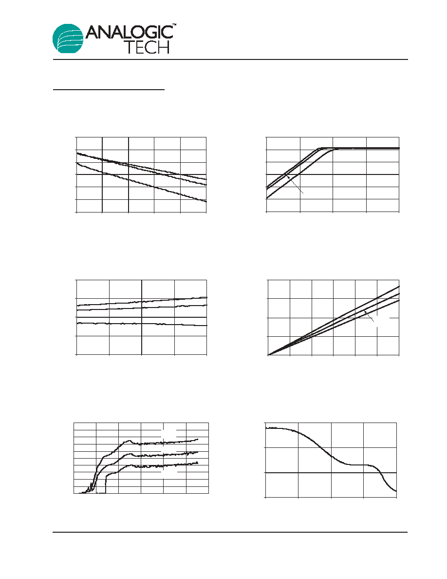
Typical Characteristics
(Unless otherwise noted, V
IN
= V
OUT
+ 1V, T
A
= 25įC, C
IN
= C
OUT
= 1ĶF ceramic)
PSRR with 10mA Load
0
20
40
60
1.E+01
1.E+02
1.E+03
1.E+04
1.E+05
Frequency (Hz)
PSRR
(
d
B
)
Supply Current vs. Input Voltage
0.0
0.2
0.4
0.6
0.8
1.0
1.2
1.4
1.6
1.8
2.0
0
1
2
3
4
5
6
Input (V)
Input (
Ķ
A) with No Load
80
į
C
25
į
C
-30
į
C
Drop-out Voltage vs. Output Current
0
100
200
300
40 0
0
25
50
75
100
125
150
Output (mA)
Drop-out
(
m
V
)
80ļC
-30ļC
25ļC
Output Voltage vs. Input Voltage
2.99
3
3.01
3.02
3.03
3.5
4
4.5
5
5.5
Input ( V )
O
u
t
p
u
t
(V)
1mA
10mA
40mA
Output Voltage vs. Input Voltage
2.5
2.6
2.7
2.8
2.9
3
3.1
2.7
2.9
3.1
3.3
3.5
Input (V)
O
u
t
p
u
t
(V)
1mA
10mA
40mA
Output Voltage vs. Output Current
2.97
2.98
2.99
3
3.01
3.02
3.03
0
20
40
60
80
100
Output (mA)
O
u
t
p
u
t
(V)
80ļC
25ļC
-30ļC

AAT3223
250mA NanoPowerTM LDO
Linear Regulator with Power OK
6
3223.2004.07.1.3
(Unless otherwise noted, V
IN
= V
OUT
+ 1V, T
A
= 25įC, C
IN
= C
OUT
= 1ĶF ceramic)
Load Transient - 1 mA / 80 mA
2
3
4
-1
0
1
2
3
Time (ms)
O
u
t
p
u
t
(V)
0
80
160
240
320
O
u
t
p
u
t
(m
A)
Output
Load Transient - 1 mA / 40 mA
2
3
4
-1
0
1
2
3
Time (ms)
O
u
t
p
u
t
(V)
0
80
160
240
320
O
u
t
p
u
t
(m
A)
Output
Line Response with 100mA Load
2.6
2.8
3
3.2
3.4
3.6
3.8
-200
0
200
400
600
800
Time (
Ķ
s)
Output
Voltage
(
V
)
0
1
2
3
4
5
6
Input
Voltage
(
V
)
Input
Output
Line Response with 10mA Load
2.6
2.8
3
3.2
3.4
3.6
3.8
-200
0
200
400
600
800
Time (
Ķ
s)
Output
Voltage
(
V
)
0
1
2
3
4
5
6
Input
Voltage
(
V
)
Input
Output
Line Response with 1mA Load
2.6
2.8
3
3.2
3.4
3.6
3.8
-200
0
200
400
600
800
Time (
Ķ
s)
Output
Voltage
(
V
)
0
1
2
3
4
5
6
Input
Voltage
(
V
)
Input
Output
Noise Spectrum
-30
-20
-10
0
10
20
30
1.E+01
1.E+02
1.E+03
1.E+04
1.E+05
1.E+06
Frequency (Hz)
Noise
(
dB
Ķ
V/
r
t
H
z
)

(Unless otherwise noted, V
IN
= V
OUT
+ 1V, T
A
= 25įC, C
IN
= C
OUT
= 1ĶF ceramic)
Turn On with 100mA Load
-1
0
1
2
3
4
5
Time (ms)
OUT (1V/div)
POK (1V/div)
EN (1V/div)
Power Up with 100mA Load
-1
0
1
2
3
4
5
Time (ms)
IN (1V/div)
OUT (1V/div)
POK (1V/div)
Turn On with 10mA Load
-1
0
1
2
3
4
5
Time (ms)
OUT (1V/div)
POK (1V/div)
EN (1V/div)
Power Up with 10mA Load
-1
0
1
2
3
4
5
Time (ms)
IN (1V/div)
OUT (1V/div)
POK (1V/div)
Turn On with 1mA Load
-1
0
1
2
3
4
5
Time (ms)
OUT (1V/div)
POK (1V/div)
EN (1V/div)
Power Up with 1mA Load
-1
0
1
2
3
4
5
Time (ms)
IN (1V/div)
OUT (1V/div)
POK (1V/div)
AAT3223
250mA NanoPowerTM LDO
Linear Regulator with Power OK
3223.2004.07.1.3
7

(Unless otherwise noted, V
IN
= V
OUT
+ 1V, T
A
= 25įC, C
IN
= C
OUT
= 1ĶF ceramic)
EN Threshold vs. V
IN
0.50
0.75
1.00
1.25
1.50
3.0
3.5
4.0
4.5
5.0
5.5
V
IN
(V)
EN Threshold (V)
-30
į
C
80
į
C
25
į
C
Current Limit Response
-200
0
200
400
600
800
1000
Time (ms)
OUT (1V/div)
POK (1V/div)
I
OUT
(200mA/div)
Power Off from 100mA Load
-1
0
1
2
3
4
5
Time (
Ķ
s)
OUT (1V/div)
POK (1V/div)
EN (1V/div)
AAT3223
250mA NanoPowerTM LDO
Linear Regulator with Power OK
8
3223.2004.07.1.3
AAT3223
250mA NanoPowerTM LDO
Linear Regulator with Power OK
3223.2004.07.1.3
9
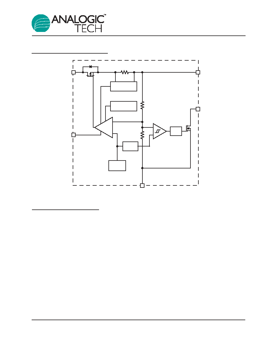
Functional Block Diagram
Over-Temperature
Protection
Over-Current
Protection
+
-
IN
EN
POK
OUT
GND
+
-
91%
V
REF
Voltage
Reference
1ms
Delay
Error
Amplifier
Functional Description
The AAT3223 is intended for LDO regulator applica-
tions where output current load requirements range
from No Load to 250mA. The advanced circuit
design of the AAT3223 has been optimized for very
low quiescent or ground current consumption making
it ideal for use in power management systems in
small battery operated devices. The typical quies-
cent current level is just 1.1ĶA. The AAT3223 also
contains an enable circuit, which has been provided
to shutdown the LDO regulator for additional power
conservation in portable products. In the shutdown
state the LDO draws less than 1ĶA from input supply.
The Power OK (POK) function has been incorpo-
rated to allow notification to application circuits
when the output voltage falls out of regulation. If
the output voltage falls below the regulation thresh-
old limit, which is compared to a level set by the
internal voltage reference, the POK pin is pulled to
ground through an N-Channel mosfet.
The LDO also demonstrates excellent power sup-
ply ripple rejection (PSRR), load and line transient
response characteristics. The AAT3223 is a truly
high performance LDO regulator especially well
suited for circuit applications which are sensitive to
load circuit power consumption and extended bat-
tery life.
The LDO regulator output has been specifically
optimized to function with low cost, low ESR
ceramic capacitors. However, the design will allow
for operation over a wide range of capacitor types.
The AAT3223 has complete short circuit and ther-
mal protection. The integral combination of these
two internal protection circuits give the AAT3223 a
comprehensive safety system to guard against
extreme adverse operating conditions. Device
power dissipation is limited to the package type
and thermal dissipation properties. Refer to the
thermal considerations discussion in the section for
details on device operation at maximum output cur-
rent loads.

AAT3223
250mA NanoPowerTM LDO
Linear Regulator with Power OK
10
3223.2004.07.1.3
Applications Information
To assure the maximum possible performance is
obtained from the AAT3223, please refer to the fol-
lowing application recommendations.
Input Capacitor
Typically a 1ĶF or larger capacitor is recommend-
ed for C
IN
in most applications. A C
IN
capacitor is
not required for basic LDO regulator operation.
However, if the AAT3223 is physically located any
distance more than a centimeter or two from the
input power source, a C
IN
capacitor will be needed
for stable operation. C
IN
should be located as
close to the device V
IN
pin as practically possible.
C
IN
values greater than 1ĶF will offer superior input
line transient response and will assist in maximiz-
ing the power supply ripple rejection.
Ceramic, tantalum or aluminum electrolytic capaci-
tors may be selected for C
IN
as there is no specific
capacitor ESR requirement. For 250mA LDO reg-
ulator output operation, ceramic capacitors are rec-
ommended for C
IN
due to their inherent capability
over tantalum capacitors to withstand input current
surges from low impedance sources such as bat-
teries in portable devices.
Output Capacitor
For proper load voltage regulation and operational
stability, a capacitor is required between pins V
OUT
and GND. The C
OUT
capacitor connection to the
LDO regulator ground pin should be made as direct
as practically possible for maximum device per-
formance. The AAT3223 has been specifically
designed to function with very low ESR ceramic
capacitors. Although the device is intended to oper-
ate with these low ESR capacitors, it is stable over
a very wide range of capacitor ESR, thus it will also
work with some higher ESR tantalum or aluminum
electrolytic capacitors. However, for best perform-
ance, ceramic capacitors are recommended.
The value of C
OUT
typically ranges from 0.47ĶF to
10ĶF, however 1ĶF is sufficient for most operating
conditions.
If large output current steps are required by an
application, then an increased value for C
OUT
should be considered. The amount of capacitance
needed can be calculated from the step size of the
change in output load current expected and the
voltage excursion that the load can tolerate.
The total output capacitance required can be cal-
culated using the following formula:
C
OUT
=
I
◊ 15ĶF
V
Where:
I = maximum step in output current
V = maximum excursion in voltage that the load
can tolerate
Note that use of this equation results in capacitor
values approximately two to four times the typical
value needed for an AAT3223 at room tempera-
ture. The increased capacitor value is recommend-
ed if tight output tolerances must be maintained
over extreme operating conditions and maximum
operational temperature excursions. If tantalum or
aluminum electrolytic capacitors are used, the
capacitor value should be increased to compen-
sate for the substantial ESR inherent to these
capacitor types.
Capacitor Characteristics
Ceramic composition capacitors are highly recom-
mended over all other types of capacitors for use
with the AAT3223. Ceramic capacitors offer many
advantages over their tantalum and aluminum elec-
trolytic counterparts. A ceramic capacitor typically
has very low ESR, is lower cost, has a smaller PCB
footprint and is non-polarized. Line and load tran-
sient response of the LDO regulator is improved by
using low ESR ceramic capacitors. Since ceramic
capacitors are non-polarized, they are less prone
to damage if connected incorrectly.
Equivalent Series Resistance (ESR): ESR is a
very important characteristic to consider when
selecting a capacitor. ESR is the internal series
resistance associated with a capacitor, which
includes lead resistance, internal connections,
capacitor size and area, material composition and
ambient temperature. Typically capacitor ESR is
measured in milliohms for ceramic capacitors and
can range to more than several ohms for tantalum
or aluminum electrolytic capacitors.
Ceramic Capacitor Materials: Ceramic capaci-
tors less than 0.1ĶF are typically made from NPO
or COG materials. NPO and COG materials are
typically tight tolerance and very stable over tem-
perature. Larger capacitor values are typically

AAT3223
250mA NanoPowerTM LDO
Linear Regulator with Power OK
3223.2004.07.1.3
11
composed of X7R, X5R, Z5U and Y5V dielectric
materials. Large ceramic capacitors, typically
greater than 2.2ĶF are often available in the low
cost Y5V and Z5U dielectrics. These two material
types are not recommended for use with LDO reg-
ulators since the capacitor tolerance can vary more
than Ī50% over the operating temperature range of
the device. A 2.2ĶF Y5V capacitor could be
reduced to 1ĶF over the full operating temperature
range. This can cause problems for circuit opera-
tion and stability. X7R and X5R dielectrics are
much more desirable. The temperature tolerance
of X7R dielectric is better than Ī15%.
Capacitor area is another contributor to ESR.
Capacitors, which are physically large in size will
have a lower ESR when compared to a smaller
sized capacitor of equivalent material and capaci-
tance value. These larger devices can also improve
circuit transient response when compared to an
equal value capacitor in a smaller package size.
Consult capacitor vendor data sheets carefully when
selecting capacitors for use with LDO regulators.
Enable Function
The AAT3223 features an LDO regulator enable /
disable function. This pin (EN) is compatible with
CMOS logic. For a logic high signal, the EN control
level must be greater then 2.0 volts. A logic low
signal is asserted when the voltage on the EN pin
falls below 0.5 volts. For example, the active high
version AAT3223 will turn on when a logic high is
applied to the EN pin. If the enable function is not
needed in a specific application, it may be tied to
the respective voltage level to keep the LDO regu-
lator in a continuously on state; e.g. the active high
version AAT3223 will tie V
IN
to EN to remain on.
Power OK Function
The Power OK (POK) function is a very useful basic
active low error flag. When the AAT3223 output
voltage level is within regulation limits, the POK out-
put pin is a high impedance and should the tied high
to the LDO output through a high value resistor,
100k
is a good resistor value for this purpose. An
internal comparator has a reference threshold set to
trigger at 10% of the nominal AAT3223 output volt-
age. If the output voltage level drops below this pre-
set threshold, the POK function will become active
and turn on an open drain N-channel Mosfet to pull
the POK output pin to ground. There is a fixed 1ms
delay circuit between the POK comparator output
and the N-Channel Mosfet gate. The purpose of the
delay is to prevent a false triggering of the POK out-
put during device turn on or during very short dura-
tion load transient events. If necessary, additional
POK flag delay can be added by placing a capacitor
in parallel with the POK pull up resistor. The addi-
tional delay time will be set by the RC time constant
the pull up resistor and parallel capacitor values.
When the AAT3223 is in the shutdown state with
the EN pin low, the POK pin becomes low imped-
ance. The LDO output will be discharged through
the high value POK pull-up resistor. When entering
the shutdown state, there is no delay associated
with the POK output; the open-drain device turns
on immediately.
This offers the added advantage of having a hard
application turn off when the LDO regulator is
turned off. This additional function has no adverse
effect on regulator turn on time.
Short Circuit Protection and Thermal
Protection
The AAT3223 is protected by both current limit and
over temperature protection circuitry. The internal
short circuit current limit is designed to activate
when the output load demand exceeds the maxi-
mum rated output. If a short circuit condition were
to continually draw more than the current limit
threshold, the LDO regulator's output voltage will
drop to a level necessary to supply the current
demanded by the load. Under short circuit or other
over current operating conditions, the output volt-
age will drop and the AAT3223's die temperature
will increase rapidly. Once the regulator's power
dissipation capacity has been exceeded and the
internal die temperature reaches approximately
140įC the system thermal protection circuit will
become active. The internal thermal protection cir-
cuit will actively turn off the LDO regulator output
pass device to prevent the possibility of over tem-
perature damage. The LDO regulator output will
remain in a shutdown state until the internal die
temperature falls back below the 140įC trip point.
The interaction between the short circuit and ther-
mal protection systems allow the LDO regulator to
withstand indefinite short circuit conditions without
sustaining permanent damage.

AAT3223
250mA NanoPowerTM LDO
Linear Regulator with Power OK
12
3223.2004.07.1.3
No-Load Stability
The AAT3223 is designed to maintain output volt-
age regulation and stability under operational no-
load conditions. This is an important characteristic
for applications where the output current may drop
to zero. An output capacitor is required for stability
under no load operating conditions. Refer to the
output capacitor considerations section for recom-
mended typical output capacitor values.
Thermal Considerations and High
Output Current Applications
The AAT3223 is designed to deliver a continuous
output load current up to 250mA under normal
operating conditions. The limiting characteristic for
the maximum output load safe operating area is
essentially package power dissipation and the
internal preset thermal limit of the device. In order
to obtain high operating currents, careful device
layout and circuit operating conditions need to be
taken into account. The following discussions will
assume the LDO regulator is mounted on a printed
circuit board utilizing the minimum recommended
footprint and the printed circuit board is 0.062inch
thick FR4 material with one ounce copper.
At any given ambient temperature (T
A
) the maxi-
mum package power dissipation can be deter-
mined by the following equation:
P
D(MAX)
= [T
J(MAX)
- T
A
] /
JA
Constants for the AAT3223 are T
J(MAX)
, the maxi-
mum junction temperature for the device which is
125įC and
JA
= 150įC/W, the package thermal
resistance. Typically, maximum conditions are cal-
culated at the maximum operating temperature
where T
A
= 85įC, under normal ambient conditions
T
A
= 25įC. Given T
A
= 85į, the maximum package
power dissipation is 267mW. At T
A
= 25įCį, the
maximum package power dissipation is 667mW.
The maximum continuous output current for the
AAT3223 is a function of the package power dissi-
pation and the input to output voltage drop across
the LDO regulator. Refer to the following simple
equation:
I
OUT(MAX)
< P
D(MAX)
/ (V
IN
- V
OUT
)
For example, if V
IN
= 5V, V
OUT
= 2.8V and T
A
= 25į,
I
OUT(MAX)
< 267mA. The output short circuit protec-
tion threshold is set between 300mA and 450mA.
If the output load current were to exceed 267mA or
if the ambient temperature were to increase, the
internal die temperature will increase. If the condi-
tion remained constant and the short circuit protec-
tion did not activate, there would be a potential
damage hazard to LDO regulator since the thermal
protection circuit will only activate after a short cir-
cuit event occurs on the LDO regulator output.
To figure what the maximum input voltage would be
for a given load current refer to the following equa-
tion. This calculation accounts for the total power
dissipation of the LDO Regulator, including that
caused by ground current.
P
D(MAX)
= (V
IN
- V
OUT
)I
OUT
+ (V
IN
x I
GND
)
This formula can be solved for V
IN
to determine the
maximum input voltage.
V
IN(MAX)
= (P
D(MAX)
+ (V
OUT
x I
OUT
)) / (I
OUT
+ I
GND
)
The following is an example for an AAT3223 set for
a 2.8 volt output:
From the discussion above, P
D(MAX)
was deter-
mined to equal 667mW at T
A
= 25įC.
V
OUT
= 2.9 volts
I
OUT
= 250mA
I
GND
= 1.1ĶA
V
IN(MAX)
=(667mW+(2.8Vx150mA))/(150mA +1.1ĶA)
V
IN(MAX)
= 9.11V
Thus, the AAT3223 can sustain a constant 2.8V
output at a 150mA load current as long as V
IN
is
9.11V at an ambient temperature of 25įC. 5.5V is
the maximum input operating voltage for the
AAT3223, thus at 25įC, the device would not have
any thermal concerns or operational V
IN(MAX)
limits.
This situation can be different at 85įC. The follow-
ing is an example for an AAT3223 set for a 2.8 volt
output at 85įC:
From the discussion above, P
D(MAX)
was deter-
mined to equal 267mW at T
A
= 85įC.
V
OUT
= 2.9 volts
I
OUT
= 150mA
I
GND
= 1.1ĶA
V
IN(MAX)
=(267mW+(2.8Vx150mA))/(150mA +1.1ĶA)
V
IN(MAX)
= 4.58V
AAT3223
250mA NanoPowerTM LDO
Linear Regulator with Power OK
3223.2004.07.1.3
13
Higher input to output voltage differentials can be
obtained with the AAT3223, while maintaining device
functions in the thermal safe operating area. To
accomplish this, the device thermal resistance must
be reduced by increasing the heat sink area or by
operating the LDO regulator in a duty cycled mode.
For example, an application requires V
IN
= 5.0V
while V
OUT
= 2.8V at a 150mA load and T
A
= 85įC.
V
IN
is greater than 4.58V, which is the maximum
safe continuous input level for V
OUT
= 2.8V at
150mA for T
A
= 85įC. To maintain this high input
voltage and output current level, the LDO regulator
must be operated in a duty cycled mode. Refer to
the following calculation for duty cycle operation:
P
D(MAX)
is assumed to be 267mW
I
GND
= 1.1ĶA
I
OUT
= 150mA
V
IN
= 5.0 volts
V
OUT
= 2.8 volts
%DC = 100(P
D(MAX)
/ ((V
IN
- V
OUT
)I
OUT
+ (V
IN
x I
GND
))
%DC=100(267mW/((5.0V-2.8V)150mA+(5.0Vx1.1ĶA))
%DC = 80.9%
For a 150mA output current and a 2.2 volt drop
across the AAT3223 at an ambient temperature of
85įC, the maximum on time duty cycle for the
device would be 80.9%.
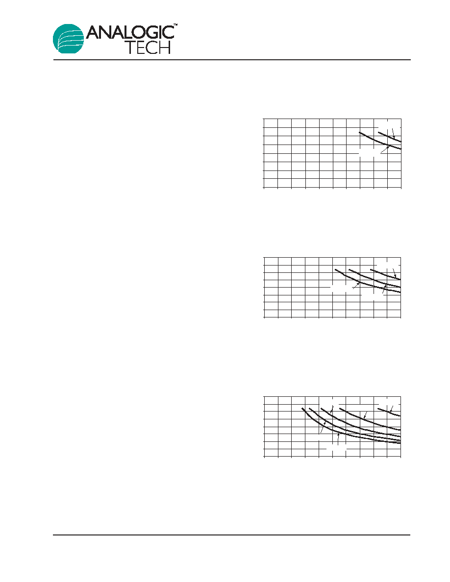
The following family of curves shows the safe oper-
ating area for duty cycled operation from ambient
room temperature to the maximum operating level.
+
Device Duty Cycle vs. V
DROP
V
OUT
= 2.8V @ 85
į
C
0
0.5
1
1.5
2
2.5
3
3.5
4
0
10
20
30
40
50
60
70
80
90
100
Duty Cycle (%)
Voltage Drop (V)
100mA
150mA
200mA
250mA
300mA
Device Duty Cycle vs. V
DROP
V
OUT
= 2.8V @ 50
į
C
0
0.5
1
1.5
2
2.5
3
3.5
4
0
10
20
30
40
50
60
70
80
90
100
Duty Cycle (%)
Voltage Drop (V)
200mA
300mA
250mA
Device Duty Cycle vs. V
DROP
V
OUT
= 2.8V @ 25
į
C
0
0.5
1
1.5
2
2.5
3
3.5
4
0
10
20
30
40
50
60
70
80
90
100
Duty Cycle (%)
Voltage Drop (V)
250mA
300mA

AAT3223
250mA NanoPowerTM LDO
Linear Regulator with Power OK
14
3223.2004.07.1.3
High Peak Output Current Applications
Some applications require the LDO regulator to
operate at continuous nominal levels with short
duration high current peaks. The duty cycles for
both output current levels must be taken into
account. To do so, one would first need to calcu-
late the power dissipation at the nominal continu-
ous level, then factor in the addition power dissipa-
tion due to the short duration high current peaks.
For example, a 2.8V system using a AAT3223IGU-
2.8-T1 operates at a continuous 100mA load cur-
rent level and has short 250mA current peaks. The
current peak occurs for 378Ķs out of a 4.61ms
period. It will be assumed the input voltage is 5.0V.
First, the current duty cycle percentage must be
calculated:
% Peak Duty Cycle: X/100 = 378ms/4.61ms
% Peak Duty Cycle = 8.2%
The LDO Regulator will be under the 100mA load
for 91.8% of the 4.61ms period and have 150mA
peaks occurring for 8.2% of the time. Next, the
continuous nominal power dissipation for the
100mA load should be determined then multiplied
by the duty cycle to conclude the actual power dis-
sipation over time.
P
D(MAX)
= (V
IN
- V
OUT
)I
OUT
+ (V
IN
x I
GND
)
P
D(100mA)
= (5.0V - 2.8V)100mA + (5.0V x 1.1ĶA)
P
D(100mA)
= 225.5mW
P
D(91.8%D/C)
= %DC x P
D(100mA)
P
D(91.8%D/C)
= 0.918 x 225.5mW
P
D(91.8%D/C)
= 207mW
The power dissipation for a 100mA load occurring
for 91.8% of the duty cycle will be 207mW. Now
the power dissipation for the remaining 8.2% of the
duty cycle at the 150mA load can be calculated:
P
D(MAX)
= (V
IN
- V
OUT
)I
OUT
+ (V
IN
x I
GND
)
P
D(250mA)
= (5.0V - 2.8V)250mA + (5.0V x 1.1ĶA)
P
D(250mA)
= 550mW
P
D(8.2%D/C)
= %DC x P
D(250mA)
P
D(8.2%D/C)
= 0.082 x 550mW
P
D(8.2%D/C)
= 45.1mW
The power dissipation for a 150mA load occurring
for 8.2% of the duty cycle will be 20.9mW. Finally,
the two power dissipation levels can summed to
determine the total true power dissipation under
the varied load.
P
D(total)
= P
D(100mA)
+ P
D(250mA)
P
D(total)
= 207mW + 45.1mW
P
D(total)
= 252.1mW
The maximum power dissipation for the AAT3223
operating at an ambient temperature of 85įC is
267mW. The device in this example will have a
total power dissipation of 252.1mW. This is within
the thermal limits for safe operation of the device.
Printed Circuit Board Layout
Recommendations
In order to obtain the maximum performance from
the AAT3223 LDO regulator, very careful attention
must be considered in regard to the printed circuit
board layout. If grounding connections are not prop-
erly made, power supply ripple rejection and LDO
regulator transient response can be compromised.
The LDO Regulator external capacitors C
IN
and
C
OUT
should be connected as directly as possible
to the ground pin of the LDO Regulator. For maxi-
mum performance with the AAT3223, the ground
pin connection should then be made directly back
to the ground or common of the source power sup-
ply. If a direct ground return path is not possible
due to printed circuit board layout limitations, the
LDO ground pin should then be connected to the
common ground plane in the application layout.
AAT3223
250mA NanoPowerTM LDO
Linear Regulator with Power OK
3223.2004.07.1.3
15
Ordering Information
Note: Sample stock is generally held on all part numbers listed in BOLD.
Note 1: XYY = assembly and date code.
Package Information
SOT23-6
1.90 BSC
0.95 BSC
0.45
Ī
0.15
0.10 BSC
2.85
Ī
0.15
0.075
Ī
0.075
0.40
Ī
0.10
◊
6
1.575
Ī
0.125
1.20
Ī
0.25
1.10
Ī
0.20
2.80
Ī
0.20
4
į
Ī
4
į
10
į
Ī
5
į
0.15
Ī
0.07
GAUGE PLANE
0.60 REF
Output Voltage
Enable
Package
Marking
1
Part Number (Tape and Reel)
1.8V
Active high
SOT23-6
EGXYY
AAT3223IGU-1.8-T1
2.7V
Active high
SOT23-6
GGXYY
AAT3223IGU-2.7-T1
2.8V
Active high
SOT23-6
EHXYY
AAT3223IGU-2.8-T1
2.8V
Active high
SC70JW-8
EHXYY
AAT3223IJS-2.8-T1
2.85V
Active high
SOT23-6
GFXYY
AAT3223IGU-2.85-T1
3.0V
Active high
SOT23-6
GEXYY
AAT3223IGU-3.0-T1
3.3V
Active high
SOT23-6
GQXYY
AAT3223IGU-3.3-T1
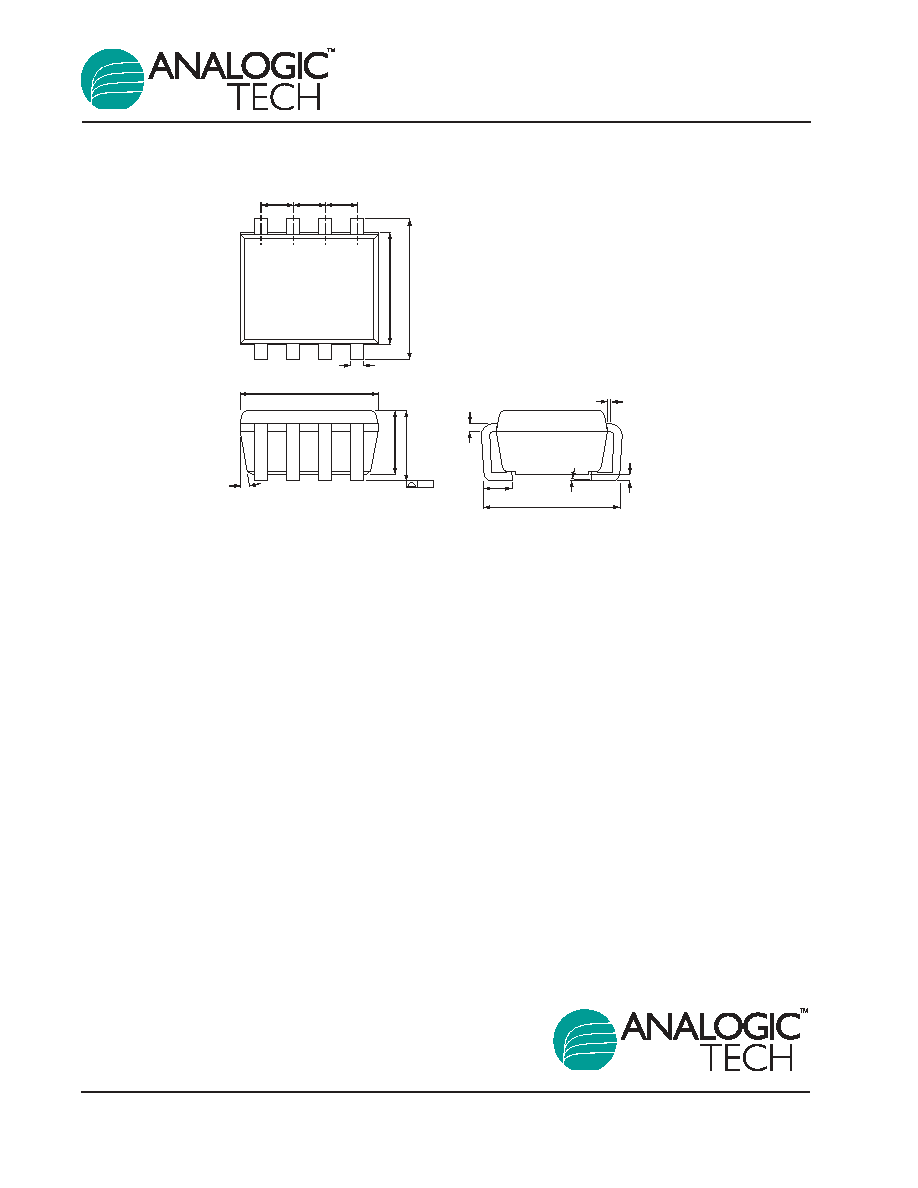
SC70JW-8
0.225
Ī
0.075
0.45
Ī
0.10
0.05
Ī
0.05
2.10
Ī
0.30
2.00
Ī
0.20
7
į
Ī
3
į
4
į
Ī
4
į
1.75
Ī
0.10
0.85
Ī
0.15
0.15
Ī
0.05
1.10 MAX
0.100
2.20
Ī
0.20
0.048REF
0.50 BSC 0.50 BSC 0.50 BSC
AAT3223
250mA NanoPowerTM LDO
Linear Regulator with Power OK
16
3223.2004.07.1.3
Advanced Analogic Technologies, Inc.
830 E. Arques Avenue, Sunnyvale, CA 94085
Phone (408) 737-4600
Fax (408) 737-4611
AnalogicTech cannot assume responsibility for use of any circuitry other than circuitry entirely embodied in an AnalogicTech product. No circuit patent licenses, copyrights, mask work
rights, or other intellectual property rights are implied.
AnalogicTech reserves the right to make changes to their products or specifications or to discontinue any product or service without notice, and advise customers to obtain the latest
version of relevant information to verify, before placing orders, that information being relied on is current and complete. All products are sold subject to the terms and conditions of sale
supplied at the time of order acknowledgement, including those pertaining to warranty, patent infringement, and limitation of liability.
AnalogicTech warrants performance of its semiconductor products to the specifications applicable at the time of sale in accordance with AnalogicTech's standard warranty. Testing and
other quality control techniques are utilized to the extent AnalogicTech deems necessary to support this warranty. Specific testing of all parameters of each device is not necessarily
performed.