11/2002
ACA2402
750/870 MHz CATV
Push-Pull Line Amplifier
PRELIMINARY DATA SHEET - Rev 1.2
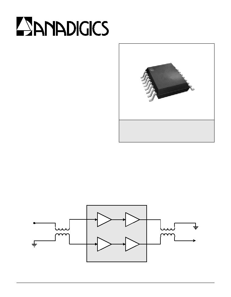
Figure 1: Hybrid Application Diagram
FEATURES
∑
22 dB Gain
∑
Very Low Distortion
∑
Excellent 75
Input and Output Match
∑
Stable with High VSWR Load Conditions
∑
Monolithic Design for Consistent Performance
Part-to-Part
∑
Low DC Power Consumption
∑
Surface Mount Package Compatible with
Automatic Assembly
∑
Low Cost Alternative to Hybrids
∑
Meets Cenelec Standards
APPLICATIONS
∑
CATV Line Amplifiers, System Amplifiers,
Distribution Nodes
S7 Package
16 Pin Wide Body SOIC
with Heat Slug
PRODUCT DESCRIPTION
The ACA2402 is a highly linear, monolithic GaAs RF
amplifier that has been developed to replace, in new
designs, standard CATV hybrid amplifiers. Offered
in a convenient surface mount package, the MMIC
consists of two pairs of parallel amplifiers that are
optimized for exceptionally low distortion and noise
figure. A hybrid equivalent that provides flat gain
response and excellent input and output return loss
over the 40 to 870 MHz CATV downstream band is
formed when one ACA2402 is cascaded between
two appropriate transmission line baluns.
RF Input
RF Output
2A
2B
1B
1A
ACA2402

2
PRELIMINARY DATA SHEET - Rev 1.2
11/2002
ACA2402
Figure 2: Pin Out
Table 1: Pin Description
1
2
3
4
5
6
7
8
16
15
14
13
12
11
10
9
GND
GND
I
SET
2A
IN
GND
2B
IN
1B
IN
1A
IN
GND
GND
1B
OUT
2B
OUT
2A
OUT
1A
OUT
Bias 1A
Bias 1B
N
I
P
E
M
A
N
N
O
I
T
P
I
R
C
S
E
D
N
I
P
E
M
A
N
N
O
I
T
P
I
R
C
S
E
D
1
D
N
G
d
n
u
o
r
G
6
1
D
N
G
d
n
u
o
r
G
2
A
2
N
I
t
u
p
n
I
A
2
r
e
if
il
p
m
A
5
1
A
1
T
U
O
t
u
p
t
u
O
A
1
r
e
if
il
p
m
A
3
D
N
G
d
n
u
o
r
G
4
1
A
1
s
a
i
B
r
e
if
il
p
m
A
A
1
r
o
f
s
a
i
B
4
A
1
N
I
t
u
p
n
I
A
1
r
e
if
il
p
m
A
3
1
A
2
T
U
O
d
n
a
t
u
p
t
u
O
A
2
r
e
if
il
p
m
A
y
l
p
p
u
S
5
B
1
N
I
t
u
p
n
I
B
1
r
e
if
il
p
m
A
2
1
B
2
T
U
O
d
n
a
t
u
p
t
u
O
B
2
r
e
if
il
p
m
A
y
l
p
p
u
S
6
I
T
E
S
t
s
u
j
d
A
t
n
e
r
r
u
C
1
1
B
1
s
a
i
B
r
e
if
il
p
m
A
B
1
r
o
f
s
a
i
B
7
B
2
N
I
t
u
p
n
I
B
2
r
e
if
il
p
m
A
0
1
B
1
T
U
O
t
u
p
t
u
O
B
1
r
e
if
il
p
m
A
8
D
N
G
d
n
u
o
r
G
9
D
N
G
d
n
u
o
r
G
PRELIMINARY DATA SHEET - Rev 1.2
11/2002
3
ACA2402
Table 2: Absolute Mimimum and Maximum Ratings
ELECTRICAL CHARACTERISTICS
Stresses in excess of the absolute ratings may cause permanent
damage. Functional operation is not implied under these conditions.
Exposure to absolute ratings for extended periods of time may
adversely affect reliability.
Table 3: Operating Ranges
Notes:
1. Pins 2, 4, 5 and 7 should be AC-coupled. No external DC bias should
be applied.
2. Pin 6 should be AC-grounded and/or pulled to ground through a resistor
for current control. No external DC bias should be applied.
3. Pins 11 and 14 are bias feeds for input amplifiers 1A and 1B. No
external DC bias should be applied.
4. Pins 10 and 15 receive DC bias directly from pins 11 and 14. No other
external bias should be applied.
The device may be operated safely over these conditions; however, parametric
performance is guaranteed only over the conditions defined in the electrical
specifications.
R
E
T
E
M
A
R
A
P
N
I
M
X
A
M
T
I
N
U
)
3
1
,
2
1
s
n
i
p
(
y
l
p
p
u
S
0
8
2
+
C
D
V
)
5
,
4
s
n
i
p
(
s
t
u
p
n
I
t
a
r
e
w
o
P
F
R
-
5
7
+
V
m
B
d
e
r
u
t
a
r
e
p
m
e
T
e
g
a
r
o
t
S
5
6
-
0
5
1
+
C
∞
e
r
u
t
a
r
e
p
m
e
T
g
n
ir
e
d
l
o
S
-
0
6
2
+
C
∞
e
m
i
T
g
n
ir
e
d
l
o
S
-
0
.
5
c
e
S
R
E
T
E
M
A
R
A
P
N
I
M
P
Y
T
X
A
M
T
I
N
U
V
:
y
l
p
p
u
S
DD
)
3
1
,
2
1
s
n
i
p
(
-
4
2
+
-
C
D
V
y
c
n
e
u
q
e
r
F
F
R
0
4
-
0
7
8
z
H
M
e
r
u
t
a
r
e
p
m
e
T
e
s
a
C
0
4
-
-
0
1
1
+
C
∞
4
PRELIMINARY DATA SHEET - Rev 1.2
11/2002
ACA2402
Table 4: AC and DC Electrical Specifications
(T
A
= +25 ∞C, V
DD
= +24 VDC)
Notes:
(1) Measured with baluns on the input and output of the device.
(2) Parts measured with 77 channels flat output, +42 dBmV per channel.
(3) Parts measured with 110 channels flat output, +40 dBmV per channel.
(4) Parts measured with 128 channels flat output, +40 dBmV per channel.
(5) The supply current may be reduced by decreasing the value of R3 (see Figure 17).
6. All specifications as measured on Evaluation Board (see Figures 16 & 17).
R
E
T
E
M
A
R
A
P
N
I
M
P
Y
T
X
A
M
T
I
N
U
S
T
N
E
M
M
O
C
z
H
M
0
7
8
@
n
i
a
G
)
1
(
3
.
1
2
8
.
1
2
3
.
2
2
B
d
e
p
o
l
S
t
n
e
l
a
v
i
u
q
E
e
l
b
a
C
)
1
(
-
0
-
B
d
s
s
e
n
t
a
l
F
n
i
a
G
)
1
(
z
H
M
0
7
8
@
-
2
.
0
±
-
B
d
e
r
u
g
i
F
e
s
i
o
N
)
1
(
-
5
.
3
0
.
4
B
d
B
T
C
)
1
(
s
l
e
n
n
a
h
C
7
7
)
2
(
s
l
e
n
n
a
h
C
0
1
1
)
3
(
s
l
e
n
n
a
h
C
8
2
1
)
4
(
-
-
-
6
7
-
3
7
-
0
7
-
4
7
-
1
7
-
-
c
B
d
O
S
C
)
1
(
s
l
e
n
n
a
h
C
7
7
)
2
(
s
l
e
n
n
a
h
C
0
1
1
)
3
(
s
l
e
n
n
a
h
C
8
2
1
)
4
(
-
-
-
2
7
-
2
7
-
9
6
-
0
7
-
0
7
-
-
c
B
d
D
O
M
X
)
1
(
s
l
e
n
n
a
h
C
7
7
)
2
(
s
l
e
n
n
a
h
C
0
1
1
)
3
(
s
l
e
n
n
a
h
C
8
2
1
)
4
(
-
-
5
6
-
5
6
-
2
6
-
3
6
-
3
6
-
-
c
B
d
)
t
u
p
t
u
O
/t
u
p
n
I
(
s
s
o
L
n
r
u
t
e
R
)
1
(
8
1
2
2
-
B
d
5
7
m
e
t
s
y
s
t
n
e
r
r
u
C
y
l
p
p
u
S
)
5
(
0
4
2
0
5
2
0
6
2
A
m
e
c
n
a
t
s
i
s
e
R
l
a
m
r
e
h
T
-
-
8
.
3
o
W
/
C

PRELIMINARY DATA SHEET - Rev 1.2
11/2002
5
ACA2402
PERFORMANCE DATA
Figure 3: Noise Figure vs. Frequency
2
2.5
3
3.5
4
4.5
5
0
100
200
300
400
500
600
700
800
900
1000
Frequency (MHz)
Noi
s
e
F
i
gur
e
(
dB)
Figure 4: Gain (S21) vs. Frequency
19
19.5
20
20.5
21
21.5
22
22.5
23
23.5
24
0
100
200
300
400
500
600
700
800
900
1000
Frequency (MHz)
Ga
in
(d
B
)