
07/2003
S24 Package
SOT-89
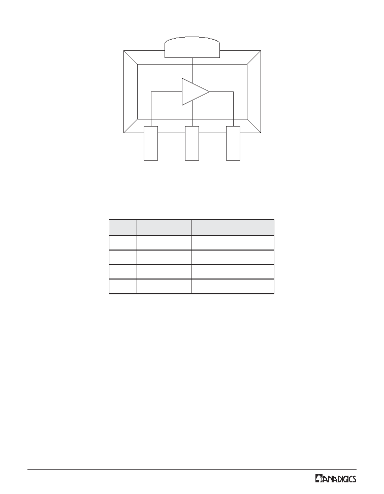
Figure 1: Block Diagram
AGB3307
50
High Linearity Low Noise
Wideband Gain Block
PRELIMINARY DATA SHEET - Rev 1.2
FEATURES
∑
DC-5500 MHz Operation Bandwidth
∑
+42 dBm Output IP3 at 850 MHz
∑
5 dB Noise Figure at 850 MHz
∑
12 dB Gain at 850 MHz
∑
+17.5 dBm P1dB at 1950 MHz
∑
SOT-89 Package
∑
Single +8 V to +12 V Supply
∑
Case Temperature: -40 to +85 ∞C
APPLICATIONS
∑
Cellular Base Stations for W-CDMA, CDMA,
TDMA, GSM, PCS and CDPD systems
∑
Fixed Wireless
∑
MMDS/WLL
∑
WLAN, HyperLAN
PRODUCT DESCRIPTION
The AGB3307 is one of a series of high performance
InGaP HBT amplifiers designed for use in
applications requiring high linearity, low noise and
low distortion. No external matching components
are needed for insertion into a 50
system. With a
high output IP3, low noise figure and wide band
operation, the AGB3307 is ideal for wireless
infrastructure applications such as Cellular Base
Stations, MMDS, and WLL. Offered in a low cost
SOT-89 surface mount package, the AGB3307
requires a single supply voltage, and typically
consumes 0.6 Watts of power using a +8 V supply.
RF Output
/ Bias
RF Input
2
PRELIMINARY DATA SHEET - Rev 1.2
07/2003
AGB3307
2
3
1
4
RF
IN
RF
OUT
GND
GND
Figure 2: Pinout (X-ray Top View)
Table 1: Pin Description
N
I
P
E
M
A
N
N
O
I
T
P
I
R
C
S
E
D
1
F
R
N
I
t
u
p
n
I
F
R
2
D
N
G
d
n
u
o
r
G
3
F
R
T
U
O
s
a
i
B
/
t
u
p
t
u
O
F
R
4
D
N
G
d
n
u
o
r
G
PRELIMINARY DATA SHEET - Rev 1.2
07/2003
AGB3307
3
ELECTRICAL CHARACTERISTICS
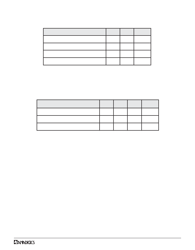
Table 2: Absolute Minimum and Maximum Ratings
Stresses in excess of the absolute ratings may cause permanent
damage. Functional operation is not implied under these conditions.
Exposure to absolute ratings for extended periods of time may
adversely affect reliability.
Table 3: Operating Ranges
The device may be operated safely over these conditions; however, parametric
performance is guaranteed only over the conditions defined in the electrical
specifications.
R
E
T
E
M
A
R
A
P
N
I
M
X
A
M
T
I
N
U
V
(
e
g
a
tl
o
V
e
c
i
v
e
D
C
C
)
0
6
+
C
D
V
P
(
r
e
w
o
P
t
u
p
n
I
F
R
N
I
)
-
0
1
+
m
B
d
T
(
e
r
u
t
a
r
e
p
m
e
T
e
g
a
r
o
t
S
G
T
S
)
0
4
-
0
5
1
+
C
∞
e
r
u
t
a
r
e
p
m
e
T
n
o
it
c
n
u
J
-
0
0
2
+
C
∞
R
E
T
E
M
A
R
A
P
N
I
M
P
Y
T
X
A
M
T
I
N
U
)
f
(
y
c
n
e
u
q
e
r
F
g
n
it
a
r
e
p
O
)
1
(
-
-
0
0
5
5
z
H
M
V
(
e
g
a
tl
o
V
y
l
p
p
u
S
Y
L
P
P
U
S
)
)
2
(
-
8
+
-
C
D
V
T
(
e
r
u
t
a
r
e
p
m
e
T
e
s
a
C
C
)
0
4
-
-
5
8
+
C
∞
Notes:
(1) Operating frequency is defined by the output return loss (S22) having a VSWR less
than 2:1.
(2) Voltage applied through a bias resistor and inductor. Refer to Figure 3. For other
supply voltages, see the APPLICATION INFORMATION section.

4
PRELIMINARY DATA SHEET - Rev 1.2
07/2003
AGB3307
Table 4: Electrical Specifications
(T
A
= +25 ∞C, V
SUPPLY
= +8 VDC, 50
System)
Notes:
(1) OIP3 is measured with two tones at 1 MHz spacing at 0 dBm output power
per tone.
(2) The value for Thermal Resistance is based on a Device Voltage (V
CC
) of
+5.0 Volts.
3. Performance as measured on ANADIGICS test fixture (see Figure 3).
Figure 3: Application Circuit (50
Terminations)
CC
AGB3307
RF Choke
DC Block
DC Block
Bypass
RF
Input
RF
Output
SUPPLY
38
W
Rs
0.01 F
m
100 nH
0.01 F
m
0.01 F
m
100 pF
10 pF
V
V
R
E
T
E
M
A
R
A
P
N
I
M
P
Y
T
X
A
M
T
I
N
U
S
(
n
i
a
G
1
2
)
z
H
M
0
5
8
z
H
M
0
5
9
1
z
H
M
0
4
1
2
z
H
M
0
5
4
2
-
-
-
-
9
.
1
1
7
.
1
1
5
.
1
1
5
.
1
1
-
-
-
-
B
d
3
P
I
t
u
p
t
u
O
)
1
(
z
H
M
0
5
8
z
H
M
0
5
9
1
z
H
M
0
4
1
2
z
H
M
0
5
4
2
-
-
-
-
9
.
1
4
+
0
.
6
3
+
6
.
5
3
+
8
.
3
3
+
-
-
-
-
m
B
d
)
B
d
1
P
(
n
o
i
s
s
e
r
p
m
o
C
B
d
1
t
u
p
t
u
O
z
H
M
0
5
9
1
-
4
.
7
1
+
-
m
B
d
e
r
u
g
i
F
e
s
i
o
N
z
H
M
0
5
8
-
5
-
B
d
(
e
c
n
a
t
s
i
s
e
R
l
a
m
r
e
h
T
C
J
)
)
2
(
-
0
4
1
-
W
/
C
∞
t
n
e
r
r
u
C
y
l
p
p
u
S
-
0
8
-
A
m
(I
CC
)

PRELIMINARY DATA SHEET - Rev 1.2
07/2003
AGB3307
5
PERFORMANCE DATA
Figure 4: Gain vs. Frequency
De-embedded 50
S-parameter
(T = +25 ∞C, V
= +5.0 V, I
= 80 mA)
W
A
CC
CC
0
5
10
15
20
25
0
1
2
3
4
5
6
7
Frequency (GHz)
Ma
g
S
21
:
G
ai
n
(
d
B
)
Figure 5: Isolation vs. Frequency
De-embedded 50
S-parameter
(T = +25 C, V
= +5.0 V, I
= 80 mA)
W
A
CC
o
CC
-50
-40
-30
-20
-10
0
0
1
2
3
4
5
6
7
Frequency (GHz)
Ma
g
S
12
:
I
so
la
t
i
o
n
(
d
B)
Figure 6: Input Return Loss vs. Frequency
De-embedded 50
S-parameter
(T = +25 C, V
= +5.0 V, I
= 80 mA)
W
A
CC
o
CC
-50
-40
-30
-20
-10
0
0
1
2
3
4
5
6
7
Frequency (GHz)
M
a
g
S
1
1
:
I
n
put
Re
tu
rn
Lo
ss
(d
B
)
Figure 7: Output Return Loss vs. Frequency
De-embedded 50
S-parameter
(T = +25 C, V
= +5.0 V, I
= 80 mA)
W
A
CC
o
CC
-50
-40
-30
-20
-10
0
0
1
2
3
4
5
6
7
Frequency (GHz)
M
a
g
S
2
2
:
O
u
t
pu
t
R
etu
r
n
L
os
s
(
dB
)