
07/2003
S24 Package
SOT-89
Figure 1: Block Diagram
AGB3310
50
High Linearity Low Noise
Internally Biased Wideband Gain Block
PRELIMINARY DATA SHEET - Rev 1.0
FEATURES
∑
On-chip Active Bias
∑
DC-3400 MHz Operation Bandwidth
∑
+37 dBm Output IP3 at 850 MHz
∑
5 dB Noise Figure at 850 MHz
∑
19 dB Gain at 850 MHz
∑
+19 dBm P1dB
∑
SOT-89 Package
∑
Single +5 V Supply
∑
Case Temperature: -40 to +85 ∞C
APPLICATIONS
∑
Cellular Base Stations for W-CDMA, CDMA,
TDMA, GSM, PCS and CDPD systems
∑
Fixed Wireless
∑
MMDS/WLL
∑
WLAN
PRODUCT DESCRIPTION
The AGB3310 is one of a series of high performance
InGaP HBT amplifiers designed for use in
applications requiring high linearity, low noise, and
low distortion. Active bias circuits on-chip eliminate
the need for external resistive feedback, and no
external matching components are needed for
insertion into a 50
system. With a high output IP3,
low noise figure, and wide band operation, the
AGB3310 is ideal for wireless infrastructure
applications such as Cellular Base Stations, MMDS,
and WLL. Offered in a low cost SOT-89 surface mount
package, the AGB3310 requires a single +5 V supply,
and typically consumes 0.4 Watts of power.
RF Output
/ Bias
RF Input
Active
Bias
PRELIMINARY DATA SHEET - Rev 1.0
07/2003
AGB3310
3
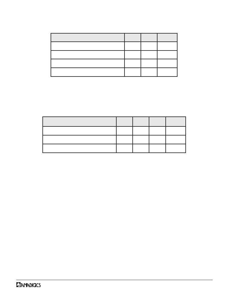
ELECTRICAL CHARACTERISTICS
Table 2: Absolute Minimum and Maximum Ratings
Stresses in excess of the absolute ratings may cause permanent
damage. Functional operation is not implied under these conditions.
Exposure to absolute ratings for extended periods of time may
adversely affect reliability.
Table 3: Operating Ranges
The device may be operated safely over these conditions; however, parametric
performance is guaranteed only over the conditions defined in the electrical
specifications.
R
E
T
E
M
A
R
A
P
N
I
M
X
A
M
T
I
N
U
V
(
e
g
a
tl
o
V
e
c
i
v
e
D
C
C
)
0
6
+
C
D
V
P
(
r
e
w
o
P
t
u
p
n
I
F
R
N
I
)
-
0
1
+
m
B
d
T
(
e
r
u
t
a
r
e
p
m
e
T
e
g
a
r
o
t
S
G
T
S
)
0
4
-
0
5
1
+
C
∞
e
r
u
t
a
r
e
p
m
e
T
n
o
it
c
n
u
J
-
0
0
2
+
C
∞
R
E
T
E
M
A
R
A
P
N
I
M
P
Y
T
X
A
M
T
I
N
U
)
f
(
y
c
n
e
u
q
e
r
F
g
n
it
a
r
e
p
O
)
1
(
-
-
0
0
4
3
z
H
M
V
(
e
g
a
tl
o
V
y
l
p
p
u
S
Y
L
P
P
U
S
)
-
5
+
-
C
D
V
T
(
e
r
u
t
a
r
e
p
m
e
T
e
s
a
C
C
)
0
4
-
-
5
8
+
C
∞
Notes:
(1) Operating frequency is defined by the output return loss (S22) having a VSWR
less than 2:1.
4
PRELIMINARY DATA SHEET - Rev 1.0
07/2003
AGB3310
Table 4: Electrical Specifications
(T
A
= +25 ∞C, V
SUPPLY
= +5 VDC, 50
system)
Notes:
(1) OIP3 is measured with two tones at 1 MHz spacing at 0 dBm output power
per tone.
2. Performance as measured on ANADIGICS test fixture (see Figure 3).
R
E
T
E
M
A
R
A
P
N
I
M
P
Y
T
X
A
M
T
I
N
U
S
(
n
i
a
G
1
2
)
z
H
M
0
5
8
z
H
M
0
5
9
1
z
H
M
0
4
1
2
z
H
M
0
5
4
2
-
-
-
-
5
.
9
1
7
1
5
.
6
1
6
1
-
-
-
-
B
d
3
P
I
t
u
p
t
u
O
)
1
(
z
H
M
0
5
8
z
H
M
0
5
9
1
z
H
M
0
4
1
2
z
H
M
0
5
4
2
-
-
-
-
7
3
+
8
3
+
9
3
+
9
3
+
-
-
-
-
m
B
d
)
B
d
1
P
(
n
o
i
s
s
e
r
p
m
o
C
B
d
1
t
u
p
t
u
O
z
H
M
0
5
8
-
9
1
+
-
m
B
d
e
r
u
g
i
F
e
s
i
o
N
z
H
M
0
5
8
-
2
.
5
-
B
d
(
e
c
n
a
t
s
i
s
e
R
l
a
m
r
e
h
T
C
J
)
-
0
4
1
-
W
/
C
∞
t
n
e
r
r
u
C
y
l
p
p
u
S
-
0
8
-
A
m
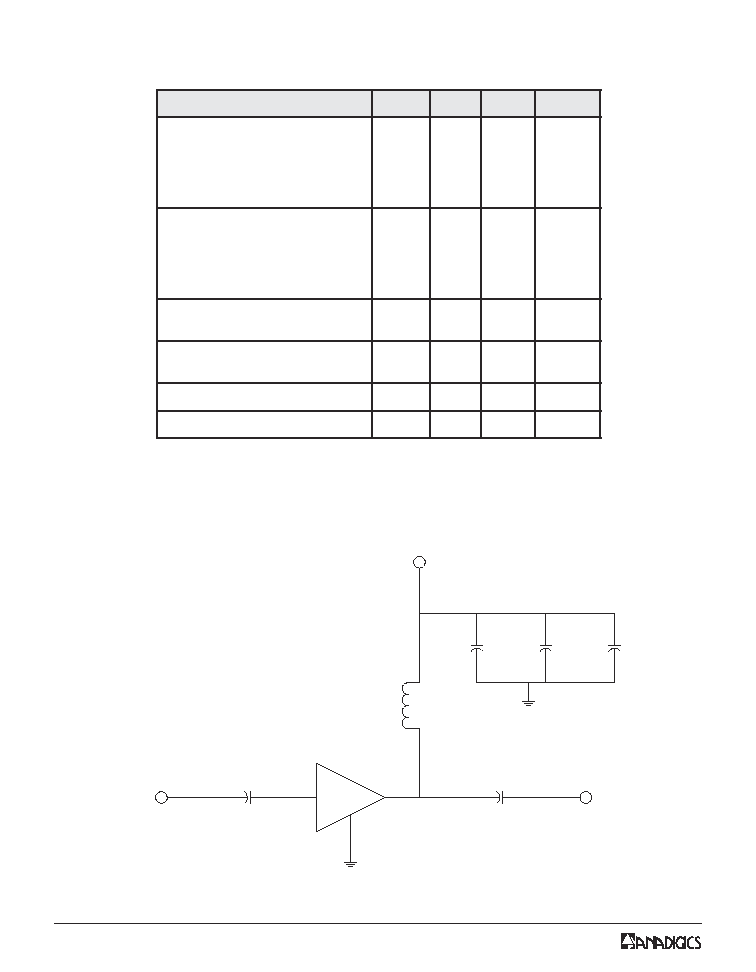
Figure 3: Application Circuit (50
Terminations)
0.01 µF
10 pF
0.01 µF
100 pF
100 nH
+5 VDC
RF Output
RF Input
AGB3310
All capacitors are muRata GRM39 series.
The inductor is a Coilcraft 0603CS series.
0.01 µF
(I
CC
)
PRELIMINARY DATA SHEET - Rev 1.0
07/2003
AGB3310
5
PERFORMANCE DATA
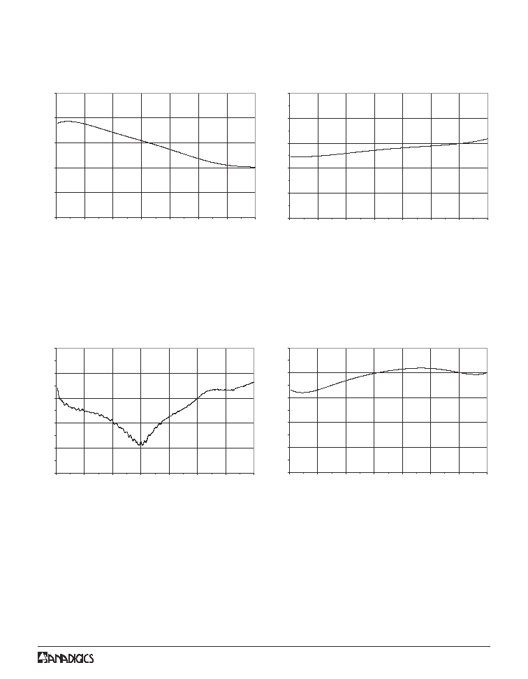
Figure 4: Gain vs. Frequency
De-embedded 50
S-parameter
(T
A
= +25 ∞C, V
SUPPLY
= +5 V, I
CC
= 80 mA)
W
0
5
10
15
20
25
0
1
2
3
4
5
6
7
Frequency (GHz)
Ma
g
S21
:
G
ai
n
(
d
B)
Figure 5: Isolation vs. Frequency
De-embedded 50
S-parameter
(T
A
= +25 ∞C, V
SUPPLY
= +5 V, I
CC
= 80 mA)
W
-50
-40
-30
-20
-10
0
0
1
2
3
4
5
6
7
Frequency (GHz)
Ma
g
S
12
:
I
so
la
t
i
o
n
(
d
B)
Figure 6: Input Return Loss vs. Frequency
De-embedded 50
S-parameter
(T
A
= +25 ∞C, V
SUPPLY
= +5 V, I
CC
= 80 mA)
W
-50
-40
-30
-20
-10
0
0
1
2
3
4
5
6
7
Frequency (GHz)
M
a
g
S
1
1
:
I
n
put
Re
tu
rn
Lo
ss
(d
B
)
Figure 7: Output Return Loss vs. Frequency
De-embedded 50
S-parameter
(T
A
= +25 ∞C, V
SUPPLY
= +5 V, I
CC
= 80 mA)
W
-50
-40
-30
-20
-10
0
0
1
2
3
4
5
6
7
Frequency (GHz)
M
ag
S
2
2:
O
u
t
pu
t
R
etu
r
n
L
os
s
(
dB
)
