
08/2001
FEATURES
∑
Single +5 Volt Supply
∑
Automatic Gain Control
∑
-31 dBm Sensitivity
∑
0 dBm Optical Overload
∑
1100 MHz Bandwidth
APPLICATIONS
∑
SONET OC-24 (1 Gb/s) Receiver
∑
Low Noise RF Amplifier
∑
BISDN
∑
HIPPI
PRODUCT DESCRIPTION
Figure 1: Equivalent Circuit
ATA12001
AGC Transimpedance Amplifier
SONET OC-24
PRELIMINARY DATA SHEET-Rev 4
D1C
The ANADIGICS ATA12001 is a 5V low noise
transimpedance amplifier with AGC designed to be
used in 1Gb/s fiber optic links. The device is used in
conjunction with a photodetector (PIN diode or
avalanche photodiode) to convert an optical signal
into an output voltage. The ATA12001 offers a
bandwidth of 1100MHz and a dynamic range of 31dB.
It is manufactured in a GaAs MESFET process and
is available in bare die form.
925 um
VDD1
I
IN
GND
GND
GND GND
GND
GND
GND
GND
C
BY
C
BY
C
AGC
V
OUT
1992
4E
1250 um
V
DD2
Photodetector Cathode must be connected to
I
IN
for proper AGC operation
V
DD2
V
OUT
C
AGC
GND
V
DD1
I
IN
C
BY
PATENT PENDING
VGA
- 35
4K
70K
4pF
+ 0.8
AGC
GND
or
neg. Supply
PRELIMINARY DATA SHEET - Rev 4
08/2001
ATA12001
2
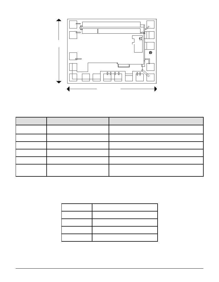
Table 1: ATA12001 Pad Description
Figure 2: Bonding Pad Layout
ELECTRICAL CHARACTERISTICS
Table 2: Absolute Maximum Ratings
D
A
P
N
O
I
T
P
I
R
C
S
E
D
T
N
E
M
M
O
C
V
1
D
D
V
1
D
D
e
g
a
t
s
n
i
a
g
t
u
p
n
i
r
o
f
y
l
p
p
u
s
e
v
it
i
s
o
P
V
2
D
D
V
2
D
D
e
g
a
t
s
n
i
a
g
d
n
o
c
e
s
r
o
f
y
l
p
p
u
s
e
v
it
i
s
o
P
I
N
I
t
n
e
rr
u
C
t
u
p
n
I
A
I
T
n
o
it
a
r
e
p
o
r
e
p
o
r
p
r
o
f
e
d
o
h
t
a
c
r
o
t
c
e
t
e
d
t
c
e
n
n
o
C
V
T
U
O
e
g
a
tl
o
V
t
u
p
t
u
O
A
I
T
k
c
o
l
b
C
D
l
a
n
r
e
t
x
e
s
e
ri
u
q
e
R
C
C
G
A
r
o
ti
c
a
p
a
C
C
G
A
l
a
n
r
e
t
x
E
C
*
K
0
7
C
G
A
t
n
a
t
s
n
o
C
e
m
i
T
C
R
C
G
A
=
C
Y
B
s
s
a
p
y
B
e
g
a
t
S
n
i
a
G
t
u
p
n
I
r
o
ti
c
a
p
a
C
F
p
6
5
>
V
1
D
D
V
0
.
7
V
2
D
D
V
0
.
7
I
N
I
A
m
5
T
A
C
∞
5
2
1
o
t
C
∞
0
4
-
.
p
m
e
T
g
n
it
a
r
e
p
O
T
S
C
∞
0
5
1
o
t
C
∞
5
6
-
.
p
m
e
T
e
g
a
r
o
t
S
925 um
VDD1
I
IN
GND
GND
GND GND
GND
GND
GND
GND
C
BY
C
BY
C
AGC
V
OUT
1992
4E
1250 um
V
DD2
Stresses in excess of the absolute ratings may cause
permanent damage. Functional operation is not implied
under these conditions. Exposure to absolute ratings
for extended periods of time may adversely affect
reliability.
PRELIMINARY DATA SHEET - Rev 4
08/2001
ATA12001
3
Table 3: Electrical Specifications
(1)
(T
A
= 25
∞
C, V
DD
=+5.0V + 10%, C
DIODE
+ C
STRAY
= 0.5 pF, Det. cathode to I
IN
)
Notes:
1. f = 50MHz
2. Measured with I
in
below AGC Threshold. During AGC, input impedance will
decrease proportionally to I
in.
3. Defined as the I
in
where Transresistance has decreased by 50%.
4. See note on Indirect Measurement of Optical Overload.
5. See note on Measurement of Input Referred Noise Current.
6. C
AGC
= 220 pF
7. Parameter is guaranteed (not tested) by design and characterization data
@ 1.2 Gb/s, assuming dectector responsivity of 0.9.
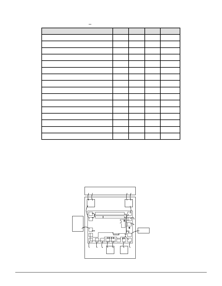
Figure 3: ATA 12001 Typical Bonding Diagram
R
E
T
E
M
A
R
A
P
N
I
M
P
Y
T
X
A
M
T
I
N
U
R
(
e
c
n
a
t
s
i
s
e
r
s
n
a
r
T
L
I,
=
C
D
)
A
n
0
0
5
<
5
.
3
K
R
(
e
c
n
a
t
s
i
s
e
r
s
n
a
r
T
L
)
0
5
=
)
1
(
2
.
1
4
.
1
K
B
d
3
-
h
t
d
i
w
d
n
a
B
0
0
9
0
0
1
1
z
H
M
e
c
n
a
t
s
i
s
e
R
t
u
p
n
I
)
2
(
0
0
1
e
c
n
a
t
s
i
s
e
R
t
u
p
t
u
O
0
3
0
5
0
6
t
n
e
rr
u
C
y
l
p
p
u
S
5
1
0
3
5
4
A
m
e
g
a
tl
o
V
t
e
s
ff
O
t
u
p
n
I
4
.
1
6
.
1
9
.
1
s
tl
o
V
e
g
a
tl
o
V
t
e
s
ff
O
t
u
p
t
u
O
8
.
1
s
tl
o
V
I(
d
l
o
h
s
e
r
h
T
C
G
A
N
I
)
)
3
(
0
0
1
0
5
1
A
d
a
o
lr
e
v
O
l
a
c
it
p
O
)
4
(
3
-
0
m
B
d
t
n
e
rr
u
C
e
s
i
o
N
t
u
p
n
I
)
5
(
0
2
1
0
7
1
A
n
t
n
a
t
s
n
o
C
e
m
i
T
C
G
A
)
6
(
6
1
c
e
s
tf
ir
D
e
g
a
tl
o
V
t
e
s
ff
O
1
±
/
V
m
C
∫
y
ti
v
it
i
s
n
e
S
l
a
c
it
p
O
)
7
(
9
2
-
1
3
-
m
B
d
e
g
n
a
R
e
g
a
tl
o
V
g
n
it
a
r
e
p
O
5
.
4
+
0
.
5
+
0
.
6
+
s
tl
o
V
e
g
n
a
R
e
r
u
t
a
r
e
p
m
e
T
g
n
it
a
r
e
p
O
0
4
-
5
8
C
∫
m
m
W
•
W
W
W
W
VDD1
I
IN
GND
GND
GND GND
GND
GND
GND
GND
C
BY
C
BY
C
AGC
V
OUT
1992
4E
V
DD2
PIN
56pF
56pF
OUT
56pF
56pF
VDD
GND

PRELIMINARY DATA SHEET - Rev 4
08/2001
ATA12001
4
Figure 4: Typical Application HIPPI 1 Gb/s
APPLICATION INFORMATION
Power Supplies and General Layout Considerations
The ATA12001D1C may be operated from a positive
supply as low as + 4.5 V and as high as + 6.0 V.
Below + 4.5 V, bandwidth, overload and sensitivity
will degrade, while at + 6.0 V, bandwidth, overload
and sensitivity improve (see Bandwidth vs.
Temperature curves). Use of surface mount
(preferably MIM type capacitors), low inductance
power supply bypass capacitors (>=56pF) are
essential for good high frequency and low noise
performance. The power supply bypass capacitors
should be mounted on or connected to a good low
inductance ground plane.
General Layout Considerations
Since the gain stages of the transimpedance
amplifier have an open loop bandwidth in excess of
1.5 GHz, it is essential to maintain good high
frequency layout practices. To prevent oscillations, a
low inductance RF ground plane should be made
available for power supply bypassing. Traces that
can be made short should be made short, and the
utmost care should be taken to maintain very low
capacitance at the photodiode-TIA interface (I
IN
), as
Figure 4: Bandwidth vs. Temperature
4pf
AV=-35
50
R
F
20pF
AGC
50
5pF
700 MHz
NOISE FILTER
0.1
µ
F
C
AGC
CBY
GND
I-IN
DET-BYP
0.4pF
CDET
20 nH
0.1
µ
F
V
DD
V
DD
0.1
µ
f
18pF
R
.01
µ
f
4K
excess capacitance at this node will cause a
degradation in bandwidth and sensitivity (see
Bandwidth vs. C
T
curves).
-40
10
60
85
V
DD
=
4.5 V
V
DD
= 5.0 V
V
DD
=
5.5 V
C
T
= 0.5 pF
B
a
nd
w
i
d
t
h (
G
H
z
)
Temperature (
O
C)
1.3
1.2
1.1
1.0
0.9

PRELIMINARY DATA SHEET - Rev 4
08/2001
ATA12001
5
Note: All performance curves are typical @ TA =25∞C
unless otherwise noted.
V
OUT
Connection
The output pad should be connected via a coupling
capacitor to the next stage of the receiver channel
(filter or decision circuits), as the output buffers are
not designed to drive a DC coupled 50 ohm load
(this would require an output bias current of
approximately 36 mA to maintain a quiescent 1.8
Volts across the output load). If V
OUT
is connected to a
high input impedance decision circuit (>500 ohms),
then a coupling capacitor may not be required,
although caution should be exercised since DC
offsets of the photo detector/TIA combination may
cause clipping of subsequent gain or decision
circuits.
Figure 5: Bandwidth vs. CT
Figure 6: Transimpedance vs. I
IN
Figure 7: Bandwidth vs. I
IN
Figure 8: V
OUT
vs. I
IN
V
DD
= 4.5 V
V
DD
= 5.0 V
V
DD
= 5.5 V
1800
1600
1400
1200
1000
800
600
0 0.2 0.4 0.6 0.8 1 1.2 1.4 1.6
BANDWIDTH vs. CT
B(3dB) A / 2
R
F
(C
N +
C
T
)
C
T
(pF)
Ba
nd
w
i
t
h
(
M
H
z
)
I
IN
Connection
(refer to the equivalent circuit diagram) Bonding the
detector cathode to I
IN
(and thus drawing current from
the ATA12001) improves the dynamic range. Although
the detector may be used in the reverse direction for
input currents not exceeding 25 mA, the specifications
for optical overload will not be met.
V
DD
= 5.5 V
V
DD
= 4.5 V
I
IN
(mA DC)
-2.2 -1.7 -1.2 -0.7 -0.2
2.0
1.8
1.6
1.4
1.2
1.0
0.8
0.6
0.4
Transimpedance (K Ohm)
I
IN
50
12001
I
V
DD
=5.5 V
I
IN
(mA DC)
- 2.2 - 1.7 - 1.2 - 0.7 - 0.2
1.7
1.6
1.5
1.4
1.3
1.2
1.1
1.0
I
BA
N
D
W
I
DT
H (GH
z
)
V
DD
=4.5 V
5
I
IN
R
F
V
DD
=4.5 V
V
DD
=5.5 V
Output Collapse
I
IN
V
OUT
I
IN
(mA DC)
heavy AGC
Linear Region
V
OU
T
(V
ol
ts)
R
f
12001
3.4
3.2
3.0
2.9
2.7
2.5
2.4
2.2
2.0
1.9
1.7
1.5
1.4
1.2
1.0
0.8
0.7
0.5
0.3
0.2
0.0
- 4
- 3
- 2
- 1