02/2006
AWL9924
2.4/5 GHz 802.11a/b/g
WLAN Power Amplifier
PRELIMINARY DATA SHEET - Rev 1.3
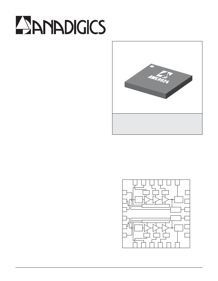
S34 Package
24 Pin 4 mm x 4 mm x 0.9 mm
LPCC
FEATURES
∑
3.8% EVM @ P
OUT
= +19 dBm with IEEE
802.11a 64 QAM OFDM at 54 Mbps
∑
3% EVM @ P
OUT
= +20 dBm with IEEE 802.11g
64 QAM OFDM at 54 Mbps
∑
-40 dBc 1st Sidelobe, -55 dBc 2nd sidelobe
ACPR at +23 dBm with IEEE 802.11b CCK/
DSSS Gaussian Filtering at 1 Mbps
∑
32 dB of Linear Power Gain at 2.4 GHz
∑
35 dB of Linear Power Gain at 5 GHz
∑
Single +3.3 V Supply
∑
Dual Temperature-Compensated Linear Power
Detectors
∑
4 mm x 4 mm x 0.9 mm LPCC Lead-Free
RoHS-Compliant Package
∑
50
- Matched RF Ports
∑
>1 kV ESD Rating (HBM)
∑
MSL 2 Rating
APPLICATIONS
∑
802.11a/b/g WLAN
PRODUCT DESCRIPTION
The ANADIGICS AWL9924 dual band power
amplifier is a high performance InGaP HBT power
amplifier IC designed for transmit applications in
the 2.4-2.5 GHz and 4.9-5.9 GHz band. Matched to
50
at all RF inputs and outputs, the part requires
no additional RF matching components off-chip,
making the AWL9924 the world's simplest dual band
PA IC implementation available. The PA exhibits
unparalleled linearity and efficiency for IEEE
802.11g, 802.11b and 802.11a WLAN systems
under the toughest signal configurations within
these standards.
The power detectors are temperature compensated
on chip, enabling separate single-ended output
voltages for each band with excellent accuracy over
a wide range of operating temperatures. The PA is
biased by a single +3.3 V supply and consumes
ultra-low current in the OFF mode.
The AWL9924 is manufactured using advanced
InGaP HBT technology that offers state-of-the-art
reliability, temperature stability and ruggedness. The
Figure 1: Block Diagram and Pinout
1
2
3
4
5
6
19
20
21
22
23
24
18
17
16
15
14
13
12
11
10
9
8
7
Input
Match
Bias
Bias
2.4 GHz PA
5 GHz PA
V
CC1
2
G
GN
D
RF O
U
T
2
G
NC
GND
DET OUT 5G
NC
GND
RF O
U
T
5
G
GN
D
V
CC1
5
G
VPC 5G
RF IN 5G
RF IN 2G
DETP 2G
VPC 2G
DETP 5G
Output
Match
Input
Match
Bias
VBC
2G
Bias
Bias
Bias
V
CC2
5
G
V
CC3
5
G
VBC
5G
Output
Match
Power
Detector
Power
Detector
V
CC2
2
G
V
CC3
2
G
Bias Control
Bias Control
DET OUT 2G
IC is provided in a 4 mm x 4 mm x 0.9 mm LPCC
package optimized for a 50
system.
4
PRELIMINARY DATA SHEET - Rev 1.3
02/2006
AWL9924
ELECTRICAL CHARACTERISTICS
Table 2: Absolute Minimum and Maximum Ratings
Stresses in excess of the absolute ratings may cause permanent damage. Functional operation is
not implied under these conditions. Exposure to absolute ratings for extended periods of time
may adversely affect reliability.
Table 3: Operating Ranges
The device may be operated safely over these conditions; however, parametric performance is
guaranteed only over the conditions defined in the electrical specifications.
Note:
(1) Applied to series resistors external to V
PC
2G and V
PC
5G pins.
R
E
T
E
M
A
R
A
P
N
I
M
P
Y
T
X
A
M
T
I
N
U
S
T
N
E
M
M
O
C
)
f
(
y
c
n
e
u
q
e
r
F
g
n
it
a
r
e
p
O
0
0
4
2
0
0
9
4
-
-
0
0
5
2
0
0
9
5
z
H
M
g
/
b
1
1
.
2
0
8
a
1
1
.
2
0
8
V
(
e
g
a
tl
o
V
y
l
p
p
u
S
1
C
C
V
,
G
2
2
C
C
,
G
2
V
3
C
C
V
,
G
2
1
C
C
V
,
G
5
2
C
C
V
,
G
5
3
C
C
)
G
5
0
.
3
+
3
.
3
+
6
.
3
+
V
V
(
e
g
a
tl
o
V
s
a
i
B
BC
V
,
G
2
C
B
)
G
5
0
.
3
+
3
.
3
+
6
.
3
+
V
s
e
ir
e
s
o
t
d
e
il
p
p
A
V
o
t
l
a
n
r
e
t
x
e
s
r
o
t
s
i
s
e
r
C
B
V
d
n
a
G
2
C
B
.
s
n
i
p
G
5
V
(
e
g
a
tl
o
V
l
o
r
t
n
o
C
r
e
w
o
P
C
P
V
,
G
2
C
P
)
G
5
-
0
3
.
3
+
-
-
5
.
0
+
V
"
N
O
"
A
P
)
1
(
"
N
W
O
D
T
U
H
S
"
A
P
)
1
(
T
(
e
r
u
t
a
r
e
p
m
e
T
e
s
a
C
C
)
0
4
-
-
5
8
+
C
∞
R
E
T
E
M
A
R
A
P
N
I
M
X
A
M
T
I
N
U
S
T
N
E
M
M
O
C
V
(
y
l
p
p
u
S
r
e
w
o
P
C
D
1
C
C
,
G
2 V
2
C
C
,
G
2
V
3
C
C
V
,
G
2
1
C
C
,
G
5 V
2
C
C
,
G
5 V
3
C
C
)
G
5
-
5
.
4
+
V
V
(
l
e
v
e
L
l
o
r
t
n
o
C
r
e
w
o
P
C
P
V
,
G
2
C
P
)
G
5
-
5
.
4
+
V
s
r
o
t
s
i
s
e
r
s
e
ir
e
s
o
t
d
e
il
p
p
A
V
o
t
l
a
n
r
e
t
x
e
C
P
V
d
n
a
G
2
C
P
G
5
.
d
e
il
p
p
a
l
a
n
g
i
s
F
R
o
N
.
s
n
i
p
V
(
l
o
r
t
n
o
C
s
a
i
B
C
B
V
,
G
2
C
B
)
G
5
-
5
.
4
+
V
s
r
o
t
s
i
s
e
r
s
e
ir
e
s
o
t
d
e
il
p
p
A
V
o
t
l
a
n
r
e
t
x
e
C
B
V
d
n
a
G
2
C
B
G
5
.
d
e
il
p
p
a
l
a
n
g
i
s
F
R
o
N
.
s
n
i
p
n
o
it
p
m
u
s
n
o
C
t
n
e
r
r
u
C
C
D
-
0
0
7
A
m
y
l
e
t
a
r
a
p
e
s
d
e
r
e
w
o
p
A
P
r
e
h
ti
E
F
R
(
l
e
v
e
L
t
u
p
n
I
F
R
N
I
F
R
,
G
2
N
I
)
G
5
-
5
-
m
B
d
e
r
u
t
a
r
e
p
m
e
T
t
n
e
i
b
m
A
g
n
it
a
r
e
p
O
0
4
-
5
8
+
C
∞
e
r
u
t
a
r
e
p
m
e
T
e
g
a
r
o
t
S
5
5
-
0
5
1
+
C
∞

PRELIMINARY DATA SHEET - Rev 1.3
02/2006
AWL9924
5
Table 4: Electrical Specifications - 2.4 GHz Continuous Wave
(T
C
= +25 ∞C, V
CC
2G = +3.3 V, V
PC
2G = +3.3 V)
Table 5: Electrical Specifications - 5 GHz Continuous Wave
(T
C
= +25 ∞C, V
CC
5G = +3.3 V, V
PC
5G = +3.3 V)
R
E
T
E
M
A
R
A
P
N
I
M
P
Y
T
X
A
M
T
I
N
U
S
T
N
E
M
M
O
C
B
d
1
P
5
.
6
2
5
.
7
2
5
.
8
2
B
d
t
n
e
r
r
u
C
n
w
o
d
t
u
h
S
-
-
5
µ
A
V
C
P
V
0
=
G
2
t
n
e
r
r
u
C
t
n
e
c
s
e
i
u
Q
0
6
0
7
0
8
A
m
V
C
P
V
,
V
3
.
3
+
=
G
2
C
C
V
3
.
3
+
=
G
2
ff
o
=
F
R
s
s
o
L
n
r
u
t
e
R
t
u
p
n
I
-
1
1
-
9
-
B
d
s
s
o
L
n
r
u
t
e
R
t
u
p
t
u
O
-
3
1
-
1
1
-
B
d
n
o
it
a
l
o
s
I
e
s
r
e
v
e
R
0
4
-
-
B
d
)
s
u
o
ir
u
p
S
(
y
ti
li
b
a
t
S
-
0
7
-
5
6
-
c
B
d
P
t
a
,
R
W
S
V
1
:
6
T
U
O
5
-
,
m
B
d
3
2
+
=
O
C
T
N
O
e
m
i
T
g
n
it
t
e
S
-
-
1
µ
S
n
i
h
ti
w
s
e
lt
t
e
S
±
B
d
5
.
0
T
F
F
O
e
m
i
T
g
n
it
t
e
S
-
-
1
µ
S
R
E
T
E
M
A
R
A
P
N
I
M
P
Y
T
X
A
M
T
I
N
U
S
T
N
E
M
M
O
C
B
d
1
P
0
.
5
2
0
.
6
2
0
.
7
2
B
d
t
n
e
r
r
u
C
n
w
o
d
t
u
h
S
-
-
5
µ
A
V
C
P
V
0
=
G
5
t
n
e
r
r
u
C
t
n
e
c
s
e
i
u
Q
0
0
1
0
2
1
5
4
1
A
m
V
C
P
V
,
V
3
.
3
+
=
G
5
C
C
V
3
.
3
+
=
G
5
ff
o
=
F
R
s
s
o
L
n
r
u
t
e
R
t
u
p
n
I
-
2
1
-
7
-
B
d
s
s
o
L
n
r
u
t
e
R
t
u
p
t
u
O
-
4
1
-
2
1
-
B
d
n
o
it
a
l
o
s
I
e
s
r
e
v
e
R
0
4
-
-
B
d
)
s
u
o
ir
u
p
S
(
y
ti
li
b
a
t
S
-
5
6
-
0
6
-
c
B
d
P
t
a
,
R
W
S
V
1
:
6
T
U
O
5
-
;
m
B
d
2
2
+
=
O
C
T
N
O
e
m
i
T
g
n
it
t
e
S
-
-
1
µ
S
n
i
h
ti
w
s
e
lt
t
e
S
±
B
d
5
.
0
T
F
F
O
e
m
i
T
g
n
it
t
e
S
-
-
1
µ
S