
08/2001
S14
SOT-6
6 Pin Plastic Package
FEATURES
Low Insertion Loss (0.4 dB @ 0.9 GHz)
Complementary Positive Control Voltages (0/
+3V to 0/+5V)
Positive Voltage Supply (+3 to +5 V)
Low DC Power Consumption
Ultra Miniature 6 Lead SOT-6 Package
Selection of Synthesizers
Filters
Amplifiers in Dual Mode & Dual Band Hand-
sets
PRODUCT DESCRIPTION
The AWS5502 is a Single Pole Double Throw GaAs
MMIC Switch assembled in a SOT-6 plastic package.
The AWS5502 is designed for analog and digital
application that require low insertion loss,
small size,
and low cost. State selection is achieved with
a complimentary positive voltage (requires positive
bias Vs, and blocking caps) or negative voltage
(no Vs or blocking caps required).
AWS5502
GaAs IC SPDT Reflective Switch
Positive Control DC - 2.5 GHz
PRELIMINARY DATA SHEET - Rev 1.0
APPLICATIONS
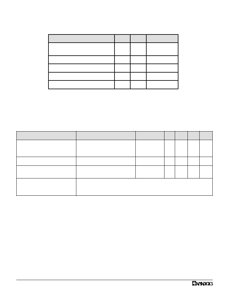
123
4
5
6
V
2
V
1
V
s
GND
RF
IN
(J1)
C
4
C
1
RF
OUT 2
(J3)
10K
C
2
RF
OUT 1
(J2)
R1
DC blocking capacitors (C
1, 2, 4
) & biasing resistor must
be supplied externally for positive voltage operation.
C
1, 2, 4
= 100 pF for operation >500 MHz.
N
I
P
N
O
I
T
C
N
U
F
N
O
I
T
P
I
R
C
S
E
D
1
)
2
J
(
T
U
O
F
R
n
a
s
a
r
o
t
u
p
n
i
n
a
s
a
d
e
s
u
e
b
n
a
c
(
tr
o
p
F
R
)t
u
p
t
u
o
2
D
N
G
s
a
tr
o
h
s
s
a
p
e
e
k
(
n
o
it
c
e
n
n
o
c
d
n
u
o
r
G
)
e
l
b
i
s
s
o
p
3
s
V
/)
1
J
(
N
I
F
R
e
v
it
i
s
o
p
r
o
f
e
g
a
tl
o
v
s
a
i
b
d
n
a
tr
o
p
n
o
m
m
o
c
F
R
)
V
5
o
t
V
3
(
l
o
rt
n
o
c
4
)
2
J
(
1
T
U
O
F
R
n
a
s
a
r
o
t
u
p
n
i
n
a
s
a
d
e
s
u
e
b
n
a
c
(
tr
o
p
F
R
)t
u
p
t
u
o
5
2
V
)
V
5
o
t
V
3
h
g
i
h
,
V
0
w
o
l(
2
e
g
a
tl
o
v
l
o
rt
n
o
C
6
1
V
)
V
5
o
t
V
3
h
g
i
h
,
V
0
w
o
l(
1
e
g
a
tl
o
v
l
o
rt
n
o
C
Figure 1: Pin Layout
Table 1: Pin Description
2
PRELIMINARY DATA SHEET - Rev 1.0
08/2001
AWS5502
Table 2: Absolute Minimum and Maximum Ratings
Stresses in excess of the absolute ratings may cause permanent
damage. Functional operation is not implied under these conditions.
Exposure to absolute ratings for extended periods of time may
adversely affect reliability.
Notes:
1. All measurements made in a 50 ohm system, unless otherwise specified.
2. DC = 300 kHz.
3. Insertion loss changes by 0.003 dB/∞C.
4. Insertion loss state.
5. Video feedthru measured wirh 1 ns rise time pulse and 500 MHz bandwidth.
ELECTRICAL CHARACTERISTICS
Table 3: Operating Ranges at 25∞ C (0, +3V)
R
E
T
E
M
A
R
A
P
N
O
I
T
I
D
N
O
C
Y
C
N
E
U
Q
E
R
F
N
I
M
P
Y
T
X
A
M
T
I
N
U
s
c
it
ir
e
t
c
a
r
a
h
C
g
n
i
h
c
ti
w
S
5
)
F
R
%
0
1
/
0
9
r
o
%
0
9
/
0
1
(
ll
a
F
,
e
s
i
R
)
F
R
%
0
1
/
%
0
9
o
t
L
T
C
%
0
5
(
ff
O
,
n
O
u
r
h
t
d
e
e
F
o
e
d
i
V
-
-
0
1
0
2
5
2
-
s
n
s
n
V
m
)
3
P
I(
t
n
i
o
P
t
p
e
c
r
e
t
n
I
n
o
it
a
l
u
d
o
m
r
e
t
n
I
m
B
d
0
1
+
r
e
w
o
P
t
u
p
n
I
e
n
o
t-
o
w
T
r
o
F
z
H
G
0
.
2
-
5
.
0
-
5
4
+
-
m
B
d
n
o
i
s
s
e
r
p
m
o
C
B
d
1
r
o
f
r
e
w
o
P
t
u
p
n
I
V
3
+
@
V
5
+
@
z
H
G
0
.
2
-
5
.
0
z
H
G
0
.
2
-
5
.
0
-
1
2
+
8
2
+
-
m
B
d
e
g
a
tl
o
V
l
o
rt
n
o
C
V
W
O
L
x
a
M
A
u
0
2
@
V
2
.
0
o
t
0
=
V
H
G
I
H
x
a
M
A
u
0
0
2
@
V
5
+
o
t
x
a
M
A
u
0
0
1
@
V
3
+
=
V
S
V
=
H
G
I
H
+
V
2
.
0
The device may be operated safely over these conditions; however, parametric performance is guaranteed
only over the conditions defined in the electrical specifications.
Q
R
E
T
E
M
A
R
A
P
N
I
M
X
A
M
T
I
N
U
r
e
w
o
P
t
u
p
n
I
F
R
l
o
rt
n
o
C
V
7
+
/
0
,
z
H
M
0
0
5
>
-
2
W
e
g
a
tl
o
V
l
o
rt
n
o
C
2
.
0
-
8
+
V
e
r
u
t
a
r
e
p
m
e
T
g
n
it
a
r
e
p
O
0
4
-
5
2
1
+
o
C
e
r
u
t
a
r
e
p
m
e
T
e
g
a
r
o
t
S
0
5
-
0
5
1
+
C
∞
C
J
-
5
2
o
W
/
C

3
PRELIMINARY DATA SHEET - Rev 1.0
08/2001
AWS5502
Table 5: Truth Table: Positive Operation
V
1
V
2
J
1
- J
2
J
1
- J
3
V
High
0
Insertion
Isolation
0
V
High
Isolation
Insertion
V
High
= +3 to +5 V (V
S
= V
High
+ 0.2 V)
Figure 2: Text Circuit Schematic
Table 4: Electrical Specifications at 25 ∞C (0, +3V)
R
E
T
E
M
A
R
A
P
1
Y
C
N
E
U
Q
E
R
F
2
N
I
M
P
Y
T
X
A
M
T
I
N
U
s
s
o
L
n
o
it
r
e
s
n
I
3
z
H
G
5
.
0
-
C
D
z
H
G
0
.
1
-
C
D
z
H
G
0
.
2
-
C
D
z
H
G
5
.
2
-
C
D
-
-
-
-
4
.
0
5
4
.
0
6
.
0
9
.
0
5
.
0
6
.
0
8
.
0
1
.
1
B
d
B
d
B
d
B
d
n
o
it
a
l
o
s
I
z
H
G
5
.
0
-
C
D
z
H
G
0
.
1
-
C
D
z
H
G
0
.
2
-
C
D
z
H
G
5
.
2
-
C
D
2
2
7
1
1
1
0
1
5
2
0
2
4
1
3
1
-
-
-
-
B
d
B
d
B
d
B
d
R
W
S
V
4
z
H
G
0
.
1
-
C
D
z
H
G
5
.
2
-
C
D
-
-
1
:
2
.
1
1
:
5
.
1
1
:
3
.
1
1
:
7
.
1
-
-

4
PRELIMINARY DATA SHEET - Rev 1.0
08/2001
AWS5502
PACKAGE OUTLINE
NOTES:
1. Package body sizes exclude mold flash and gate burrs.
2. Dimension L is measured in gage plane
3. Coplanarity: 0.1000 mm
4. Tolerance + 0.1000 mm (4 mil) unless otherwise specified.
0.10
---
0.00
A1
2.60
1∞
0.37
1.40
2.70
0.10
0.35
0.70
1
D
H
L
e
E
b
C
A2
5∞
9∞
2.90
2.80
1.90(TYP)
---
1.60
0.15
0.40
0.80
3.10
3.00
---
1.80
0.50
0.25
0.90
DIMENSIONS IN MILLIMETERS
1.00
MIN
SYMBOLS
A
1.10
NOM
MAX
1.30
MAX
0.051
0.122
0.118
---
0.071
0.020
0.010
0.035
0.004
5∞
9∞
1∞
DIMENSIONS IN INCHES
0.075(TYP)
0.00
0.102
0.015
0.055
0.106
0.004
0.014
0.027
0.039
MIN
---
0.063
0.110
---
0.114
0.006
0.016
0.031
0.043
NOM
Figure 3: S14 Package Outline

5
PRELIMINARY DATA SHEET - Rev 1.0
08/2001
AWS5502
NOTES