 | –≠–ª–µ–∫—Ç—Ä–æ–Ω–Ω—ã–π –∫–æ–º–ø–æ–Ω–µ–Ω—Ç: AWS5518 | –°–∫–∞—á–∞—Ç—å:  PDF PDF  ZIP ZIP |

03-2002
S14
SOT-26
6 Pin Plastic Package
FEATURES
∑
High Linearity (IP3 48 dBm @ 0.9 GHz)
∑
Low Insertion Loss (0.4 dB @ 0.9 GHz)
∑
2.7 V to 6 V Operation
∑
Low DC Power Consumption
∑
Ultra Miniature SOT-26 Package
∑
High Isolation
AWS5518
GaAs IC
SPDT Reflective Switch DC-2.0 GHz
PRELIMINARY DATA SHEET - Rev 1.0
PRODUCT DESCRIPTION
The AWS5518 is a Single Pole Double Throw (SPDT)
GaAs MMIC switch assembled in a SOT-26 plastic
package. The AWS5518 is designed for applications
APPLICATIONS
∑
Transmit/Receive Switch
∑
Diversity Switching
∑
Antenna Selection
Notes:
1. DC blocking capacitors C1,2,3 and optional resistor Rs
must be supplied externally.
2. C1,2,3 = 100 pF for operation >500 MHz.
3. The use of resistor Rs to the positive voltage supply is
optional. It is only required if it is necessary to independently
control the RF ports, such as selecting both ports to be OFF
at the same time.
Figure 1: Pinout Diagram
Table 1: Pin Description
1
2
3
4
5
6
GND
V1
V2
Vs
Optional Rs
see Note 3
C
3
C
2
C
1
RF
OUT1
(J2)
RF
OUT2
(J3)
RF
IN
(J1)
N
I
P
E
M
A
N
N
O
I
T
P
I
R
C
S
E
D
1
F
R
2
T
U
O
)
3
J
(
)
t
u
p
t
u
o
n
a
s
a
r
o
t
u
p
n
i
n
a
s
a
d
e
s
u
e
b
n
a
c
(
t
r
o
p
F
R
2
D
N
G
)
e
l
b
i
s
s
o
p
s
a
t
r
o
h
s
s
a
p
e
e
k
(
n
o
it
c
e
n
n
o
c
d
n
u
o
r
G
3
F
R
1
T
U
O
)
2
J
(
)
t
u
p
u
o
n
a
r
o
t
u
p
n
i
n
a
s
a
d
e
s
u
e
b
n
a
c
(
t
r
o
p
F
R
4
1
V
)
V
5
o
t
V
7
.
2
h
g
i
H
,
V
0
w
o
L
(
1
e
g
a
tl
o
v
l
o
r
t
n
o
C
5
F
R
N
I
s
V
/
)
1
J
(
e
v
it
i
s
o
p
r
o
f
e
g
a
tl
o
v
s
a
i
b
d
n
a
t
r
o
p
n
o
m
m
o
c
F
R
)
V
5
o
t
V
3
(
l
o
r
t
n
o
c
6
2
V
)
V
5
o
t
V
7
.
2
h
g
i
H
,
V
0
w
o
L
(
2
e
g
a
tl
o
v
l
o
r
t
n
o
C
that require low insertion loss, high isolation, high
linearity, and small size. The switch can be controlled
with positive, negative, or a combination of both voltages.

PRELIMINARY DATA SHEET - Rev 1.0
03/2002
AWS5518
2
Table 2: Absolute Minimum and Maximum Ratings
Table 3: Operating Ranges at 25∞ C
Notes:
1. All measurements made in a 50 Ohm system, unless other specified.
(2) Video feedthru measured with 1 ns rise time pulse and 500 MHz bandwidth.
(3) VCTL is the absolute value of the differential voltage from V1 to V2. Changing polarity selects the switch path as defined
in the truth table below. Use of the optional resistor Rs on the common port limits VHIGH to Vs ±0.2 V.
ELECTRICAL CHARACTERISTICS
The device may be operated safely over these conditions; however, parametric performance is guaranteed only over
the conditions defined in the electrical specifications.
Stresses in excess of the absolute ratings may cause permanent damage.
Functional operation is not implied under these conditions. Exposure to
absolute ratings for extended periods of time may adversely affect reliability.
R
E
T
E
M
A
R
A
P
N
I
M
X
A
M
T
I
N
U
r
e
w
o
P
t
u
p
n
I
F
R
l
o
r
t
n
o
C
V
,
z
H
M
0
0
9
>
-
6
W
e
g
a
tl
o
V
l
o
r
t
n
o
C
2
.
0
-
8
+
V
e
r
u
t
a
r
e
p
m
e
T
g
n
it
a
r
e
p
O
∞
0
4
-
5
8
+
C
∞
e
r
u
t
a
r
e
p
m
e
T
e
g
a
r
o
t
S
5
6
-
0
5
1
+
C
∞
C
J
-
∞
5
2
W
/
C
R
E
T
E
M
A
R
A
P
N
O
I
T
I
D
N
O
C
Y
C
N
E
U
Q
E
R
F
N
I
M
P
Y
T
X
A
M
T
I
N
U
s
c
it
ir
e
t
c
a
r
a
h
C
g
n
i
h
c
ti
w
S
)
2
(
)
F
R
%
0
1
/
0
9
r
o
%
0
9
/
0
1
(
ll
a
F
,
e
s
i
R
)
F
R
%
0
1
/
0
9
o
t
L
T
C
%
0
5
(
ff
O
,
n
O
u
r
h
t
d
e
e
F
o
e
d
i
V
0
0
1
0
0
1
0
0
1
S
n
S
n
V
m
)
3
P
I
(
t
n
i
o
P
t
p
e
c
r
e
t
n
I
n
o
it
a
l
u
d
o
m
r
e
t
n
I
m
B
d
7
2
o
t
m
B
d
3
1
s
l
e
v
e
l
r
e
w
o
p
e
n
o
t
-
2
)
t
s
e
t
f
o
e
g
n
a
r
c
i
m
a
n
y
d
e
z
i
m
it
p
o
o
t
d
e
t
c
e
l
e
s
(
V
L
T
C
V
7
.
2
=
V
L
T
C
V
0
.
5
=
z
H
G
0
.
1
z
H
G
8
.
1
z
H
G
0
.
1
z
H
G
8
.
1
5
4
+
2
4
+
5
5
+
2
5
+
8
4
+
6
4
+
1
6
+
6
5
+
m
B
d
m
B
d
m
B
d
m
B
d
n
o
i
s
s
e
r
p
m
o
C
B
d
1
r
o
f
r
e
w
o
p
t
u
p
n
I
V
L
T
C
V
7
.
2
=
V
L
T
C
V
0
.
5
=
z
H
G
0
.
1
z
H
G
8
.
1
z
H
G
0
.
1
z
H
G
8
.
1
8
2
+
7
2
+
7
3
+
7
3
+
m
B
d
m
B
d
m
B
d
m
B
d
l
e
v
e
L
c
i
n
o
m
r
a
H
V
,
m
B
d
0
3
+
=
r
e
w
o
p
t
u
p
n
I
L
T
C
V
0
.
5
=
z
H
G
8
.
1
&
1
5
7
-
c
B
d
V
(
e
g
a
tl
o
V
l
o
r
t
n
o
C
L
T
C
)
)
3
(
e
g
a
tl
o
v
n
o
it
a
r
e
p
o
l
a
n
i
m
o
N
7
.
2
6
V
t
n
e
r
r
u
C
e
g
a
k
a
e
L
V
L
T
C
V
7
.
2
=
V
L
T
C
V
0
.
5
=
0
5
5
7
A
µ
A
µ

PRELIMINARY DATA SHEET - Rev 1.0
03/2002
AWS5518
3
Table 5: Truth Table
Positive Operation
V
High
= 2.7 to 5 V (Vs = V
High
± 0.2 V
)
Table 4: Electrical Specifications at 25 ∞C
(VCTL = 2.7 V)
Notes:
(1) All measurements made in a 50
system, unless other specified.
(2) DC = 300 kHz
(3) In low insertion loss path.
R
E
T
E
M
A
R
A
P
( )
1
Y
C
N
E
U
Q
E
R
F
)
2
(
N
I
M
P
Y
T
X
A
M
T
I
N
U
s
s
o
L
n
o
it
r
e
s
n
I
)
3
(
z
H
G
0
.
1
-
C
D
z
H
G
0
.
2
-
C
D
5
3
.
0
5
4
.
0
5
4
.
0
5
5
.
0
B
d
n
o
it
a
l
o
s
I
z
H
G
0
.
1
-
C
D
z
H
G
0
.
2
-
C
D
5
2
2
2
2
3
4
2
B
d
R
W
S
V
)
3
(
z
H
G
0
.
2
-
5
.
0
1
:
4
.
1
B
d
1
V
2
V
1
J
2
J
-
3
J
-
1
J
V
h
g
i
H
V
w
o
L
n
o
it
a
l
o
s
I
s
s
o
L
w
o
L
V
w
o
L
V
h
g
i
H
s
s
o
L
w
o
L
n
o
it
a
l
o
s
I
PRELIMINARY DATA SHEET - Rev 1.0
03/2002
AWS5518
4
0.0
0.1
0.2
0.3
0.4
0.5
0.6
0.7
0.8
0.9
1.0
0.5
1.0
1.5
2.0
2.5
Frequency (GHz)
Ins
e
r
t
ion
Los
s
(
dB
)
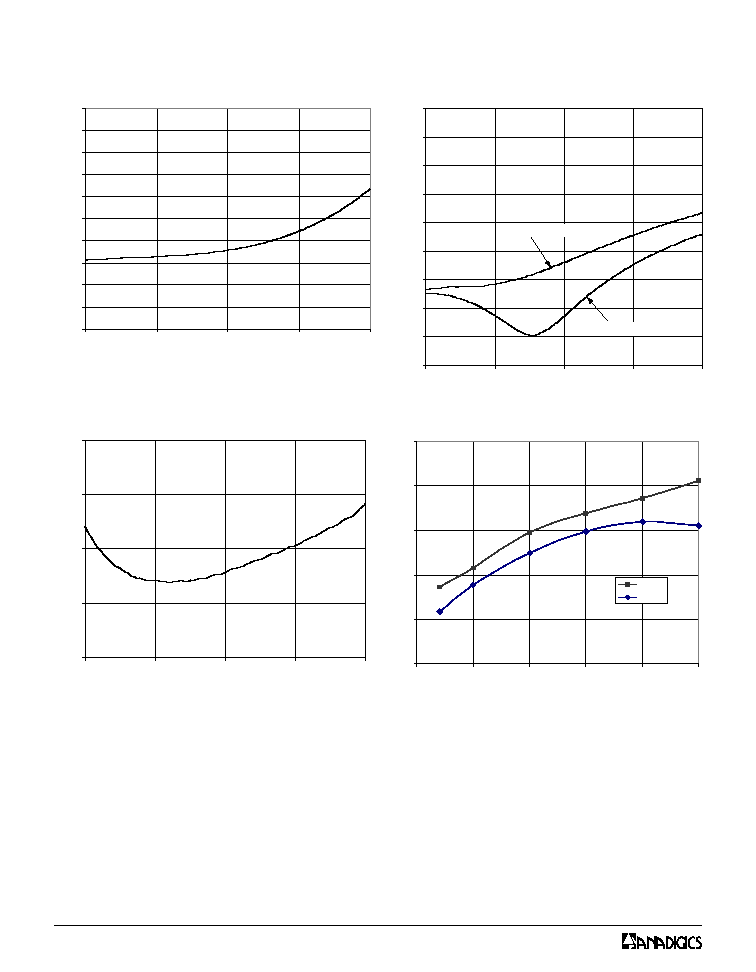
Figure 2: Insertion Loss vs. Frequency
PERFORMANCE DATA
1.0
1.1
1.2
1.3
1.4
0.5
1.0
1.5
2.0
2.5
Frequency (GHz)
VSW
R
Figure 4: VSWR vs. Frequency
40
45
50
55
60
65
2.5
3
3.5
4
4.5
5
Control Voltage (V)
TOI
(
dB
m
)
1.0GHz
1.8GHz
Figure 5: TOI vs. Control Voltage
Isolation vs Frequency
-45
-40
-35
-30
-25
-20
-15
-10
-5
0
0.5
1.0
1.5
2.0
2.5
Frequency (GHz)
Is
ola
t
ion
(
dB
)
Input to Output Isolation
Output to Output
Isolation
Figure 3: Isolation vs. Frequency
PRELIMINARY DATA SHEET - Rev 1.0
03/2002
AWS5518
5
PACKAGE OUTLINE
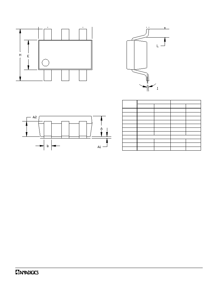
Figure 6: S14 Package Outline Diagram
NOTE
1. PACKAGE BODY SIZES EXCLUDE MOLD FLASH
AND GATE BURRS
2. DIMENSION L IS MEASURED IN GAGE PLANE
3. COPLANARITY : 0.1000 mm
4. TOLERANCE ±0.1000 mm(4 mil) UNLESS
OTHERWISE SPECIFIED
q
0.10
0.00
A1
2.60
1∞
0.37
1.40
2.70
0.10
0.35
0.70
q1
D
H
L
e
E
b
C
A2
9∞
1.90(TYP)
3.10
3.00
---
1.80
0.50
0.25
0.90
DIMENSIONS IN MILLIMETERS
1.00
MIN
SYMBOLS
A
MAX
1.30
MAX
0.051
0.122
0.118
---
0.071
0.020
0.010
0.035
0.004
9∞
1∞
DIMENSIONS IN INCHES
0.075(TYP)
0.00
0.102
0.015
0.055
0.106
0.004
0.014
0.027
0.039
MIN

PRELIMINARY DATA SHEET - Rev 1.0
03/2002
AWS5518
6
NOTES

PRELIMINARY DATA SHEET - Rev 1.0
03/2002
AWS5518
7
NOTES

PRELIMINARY DATA SHEET - Rev 1.0
03/2002
AWS5518
IMPORTANT NOTICE
ANADIGICS, Inc. reserves the right to make changes to its products or to discontinue any product at any time without notice.
The product specifications contained in Advanced Product Information sheets and Preliminary Data Sheets are subject to
change prior to a product's formal introduction. Information in Data Sheets have been carefully checked and are assumed to be
reliable; however, ANADIGICS assumes no responsibilities for inaccuracies. ANADIGICS strongly urges customers to verify
that the information they are using is current before placing orders.
WARNING
ANADIGICS products are not intended for use in life support appliances, devices, or systems. Use of an ANADIGICS product
in any such application without written consent is prohibited.
ANADIGICS, Inc.
35 Technology Drive
Warren, New Jersey 07059
Tel: +1 (908) 668-5000
Fax: +1 (908) 668-5132
URL: http://www.anadigics.com
E-mail: Mktg@anadigics.com
8
ORDERING INFORMATION
R
E
B
M
U
N
R
E
D
R
O
N
O
I
T
P
I
R
C
S
E
D
E
G
A
K
C
A
P
G
N
I
G
A
K
C
A
P
T
N
E
N
O
P
M
O
C
4
1
S
8
1
5
5
S
W
A
4
1
S
e
g
a
k
c
a
P
c
it
s
a
l
P
n
i
P
6