08/2001
9.2x11.6 mm
MCM Module Package
FEATURES
∑
InGaP HBT Technology
∑
High Efficiency 55% EGSM
∑
High Efficiency 50% DCS
∑
Low Leakage Current (5mA)
∑
SMT Module Package
∑
Small Footprint (9.2mm X 11.6mm)
∑
Low Profile (1.55 mm)
∑
50W Input and Output Matching
∑
Minimal Number of External Components
∑
GPRS Capable (2 TX Slots)
APPLICATIONS
∑
EGSM/DCS Dual Band Handsets/PDA
∑
GPRS Class 10
AWT6107
EGSM/DCS Dual Band
3.5V GPRS Power Amplifier Module
ADVANCED PRODUCT INFORMATION - Rev 0.2
PRODUCT DESCRIPTION
The AWT6107 power amplifier module has been
optimized for dual band operation (EGSM and
DCS1800 bands). The amplifier is suitable for class
10 GPRS (2 TX Slots) handsets and similar
communication systems. The module integrates
practically all circuitry associated with the power
amplifier function including bias management and
matching components for 50W systems. The bias
management includes VAPC over voltage protection
making the amplifier extremely rugged. The maximum
Figure 1: Block Diagram
output power is achieved at a lower control voltage
avoiding the need to use rail to rail operational
amplifiers in the power control scheme.
The module uses a two-stage EGSM power amplifier
and a three stage DCS1800 power amplifier. Both
power amplifier outputs have V
CC
present at the output
and require DC blocks when interfacing with other
circuitry. The input signals have internal DC blocking
and require no additional components.
Bias
controller
EGSM
IN
V
APC
V
BAND
DCS
IN
DCS
OUT
EGSM
OUT
3
ADVANCED PRODUCT INFORMATION - Rev 0.2
08/2001
AWT6107
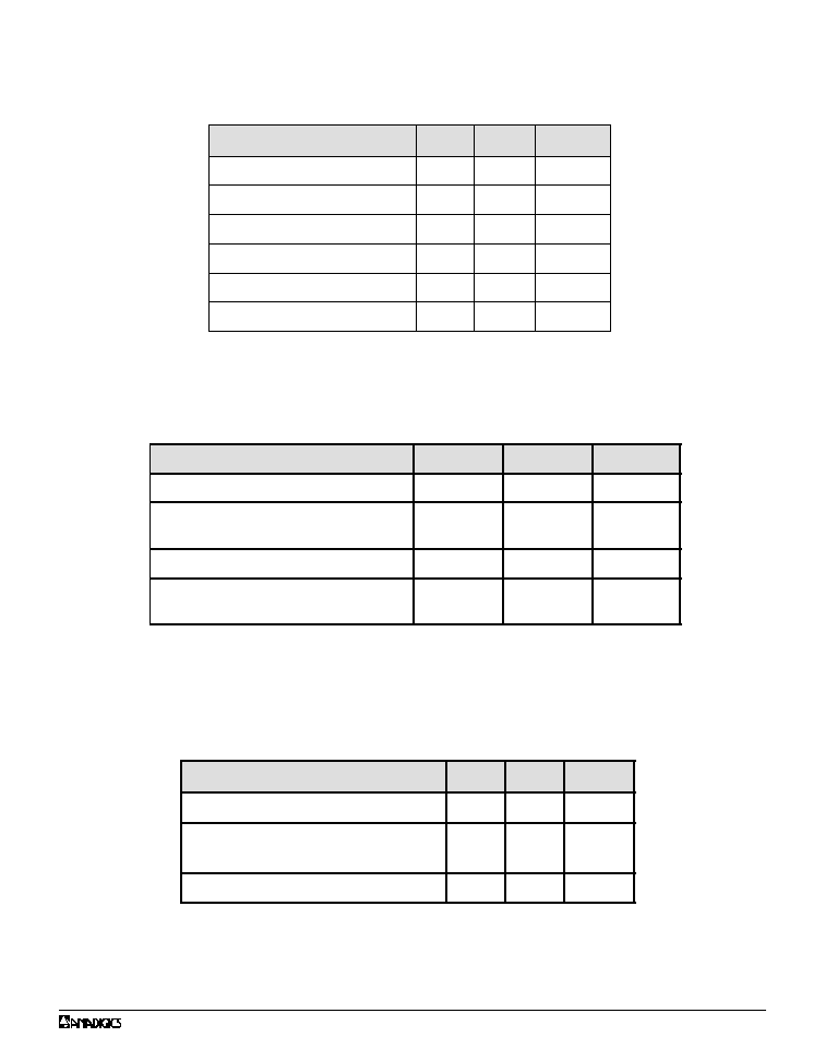
Table 2: Absolute Minimum and Maximum Ratings
Although protection circuitry has been designed into this device, proper
precautions should be taken to avoid exposure to electrostatic discharge (ESD)
during handling and mounting. Human body model HBM employed is resistance
= 1500W, capacitance = 100pF.
Table 3: ESD Ratings
Table 4: Operating Conditions
R
E
T
E
M
A
R
A
P
N
I
M
X
A
M
S
T
I
N
U
(
e
g
a
tl
o
V
y
l
p
p
u
S
V
C
C
)
7
+
V
(
r
e
w
o
P
t
u
p
n
I
F
R
N
I
)
5
1
+
m
B
d
(
e
g
a
tl
o
V
l
o
rt
n
o
C
V
C
P
A
)
V
3
.
4
+
V
(
e
r
u
t
a
r
e
p
m
e
T
e
g
a
r
o
t
S
T
G
T
S
)
5
5
-
0
5
1
C
∞
T
(
e
r
u
t
a
r
e
p
m
e
T
g
n
it
a
r
e
p
O
C
)
5
2
-
5
8
C
∞
e
r
u
t
a
r
e
p
m
e
T
w
o
lf
e
R
m
u
m
i
x
a
M
5
3
2
C
∞
Stresses in excess of the absolute ratings may cause
permanent damage. Functional operation is not implied under
these conditions. Exposure to absolute ratings for extended
periods of time may adversely affect reliability.
R
E
T
E
M
A
R
A
P
D
O
H
T
E
M
G
N
I
T
A
R
T
I
N
U
)
s
tr
o
P
F
R
(
e
g
a
tl
o
V
d
l
o
h
s
e
r
h
T
D
S
E
M
B
H
D
B
T
V
l
o
rt
n
o
C
(
e
g
a
tl
o
V
d
l
o
h
s
e
r
h
T
D
S
E
)
s
t
u
p
n
I
M
B
H
D
B
T
V
)
s
t
u
p
n
I
F
R
(
e
g
a
tl
o
V
d
l
o
h
s
e
r
h
T
D
S
E
M
D
C
D
B
T
V
l
o
rt
n
o
C
(
e
g
a
tl
o
V
d
l
o
h
s
e
r
h
T
D
S
E
)
s
t
u
p
n
I
M
D
C
D
B
T
V
The device may be operated safely over these conditions; however,
parametric performance is guaranteed only over the conditions
defined in the electrical specifications.
ELECTRICAL CHARACTERISTICS
R
E
T
E
M
A
R
A
P
N
I
M
X
A
M
S
T
I
N
U
(
e
g
a
tl
o
V
y
l
p
p
u
S
V
C
C
)
0
.
3
5
.
4
V
t
n
e
rr
u
C
e
g
a
k
a
e
L
(V
C
C
V
,
V
5
.
4
=
C
P
A
)
V
0
=
0
0
5
A
T
(
e
r
u
t
a
r
e
p
m
e
T
g
n
it
a
r
e
p
O
C
)
0
2
-
5
7
C
∞
m

4
AWT6107
ADVANCED PRODUCT INFORMATION - Rev 0.2
08/2001
EGSM:
Test Conditions: V
CC
= 3.5V, Z
IN
= Z
OUT
= 50W, T
C
= 25∞C
±
3, P
IN
= 10dBm, P
WIDTH
= 1154ms, Duty Cycle =
25%, V
BAND
= LOW
Table 6: EGSM Electrical Specification
Table 5: Operating Conditions
Power Control
Unless otherwise specified: V
CC
= 3.5V, Z
IN
= Z
OUT
= 50W, T
C
= 25∞C
±
3,
Pulse Width = 1154ms, Duty Cycle = 25%
L
A
N
G
I
S
N
I
M
X
A
M
S
T
I
N
U
(
e
g
a
tl
o
V
l
o
rt
n
o
C
V
C
P
A
)
0
0
.
3
V
I(
t
n
e
r
r
u
C
l
o
rt
n
o
C
C
P
A
)
0
1
.
0
A
m
T
(
e
r
u
t
a
r
e
p
m
e
T
g
n
it
a
r
e
p
O
C
)
0
2
-
5
7
C
∞
R
E
T
E
M
A
R
A
P
L
O
B
M
Y
S
N
I
M
P
Y
T
X
A
M
S
T
I
N
U
y
c
n
e
u
q
e
r
F
f
O
0
8
8
5
1
9
z
H
M
P
r
o
f
e
g
a
tl
o
V
l
o
rt
n
o
C
X
A
M
V
C
P
A
8
.
1
2
.
2
V
r
e
w
o
P
t
u
p
n
I
P
N
I
8
0
1
2
1
m
B
d
P
(
r
e
w
o
P
t
u
p
t
u
O
N
I
)
m
B
d
0
1
=
P
T
U
O
5
.
4
3
m
B
d
y
c
n
e
i
c
if
f
E
d
e
d
d
A
r
e
w
o
P
E
A
P
5
5
%
r
e
w
o
P
t
u
p
t
u
O
d
e
d
a
r
g
e
D
V
C
C
V
,
V
0
.
3
=
C
P
A
,
V
2
.
2
=
P
N
I
T
,
m
B
d
8
=
C
C
∞
5
7
=
2
3
m
B
d
r
e
w
o
P
t
u
p
t
u
O
.
n
i
M
/
n
o
it
a
l
o
s
I
V
C
P
A
P
,
V
2
.
0
=
N
I
m
B
d
2
1
=
P
N
I
M
0
3
-
m
B
d
c
i
n
o
m
r
a
H
2
d
n
3
d
r
z
H
G
5
7
.
2
1
o
t
o
f
4
7
-
7
-
7
-
m
B
d
m
B
d
m
B
d
R
W
S
V
1
:
5
d
a
o
L
:
y
ti
li
b
a
t
S
s
e
l
g
n
a
e
s
a
h
p
ll
A
6
3
-
m
B
d
P
:
s
s
e
n
d
e
g
g
u
R
N
I
,
m
B
d
2
1
=
V
C
C
V
,
V
5
.
4
=
C
P
A
V
0
.
3
-
2
.
0
=
1
:
8
R
W
S
V
ll
A
s
e
s
a
h
P
z
H
M
0
2
+
o
f
r
e
w
o
P
e
s
i
o
N
5
8
-
9
7
-
0
0
1
/
m
B
d
z
H
k
P
e
m
i
T
g
n
i
h
c
ti
w
S
T
U
O
o
t
m
B
d
0
1
-
=
m
B
d
5
.
4
3
+
2
s
V
(
n
o
it
i
d
n
o
C
R
W
S
V
t
u
p
n
I
C
P
A
)
V
2
.
2
=
1
:
2
1
:
5
.
2
o
it
a
R
t
u
p
t
u
o
S
C
D
t
a
r
e
w
o
p
c
i
n
o
m
r
a
H
d
n
2
0
2
-
m
B
d
m

5
ADVANCED PRODUCT INFORMATION - Rev 0.2
08/2001
AWT6107
Table 7: DCS Electrical Specification
DCS:
Test Conditions: V
CC
= 3.5V, Z
IN
= Z
OUT
= 50W, T
C
= 25∞C
±
3, P
IN
= 8dBm, P
WIDTH
= 1154ms, Duty
Cycle = 25%, V
BAND
= HIGH
Table 8: Logic Level Definitions
Logic Level Definitions:
The band select pin (V
BAND
) is used to select which amplifier is enabled by
the voltage applied to the V
APC
input.
m
R
E
T
E
M
A
R
A
P
N
I
M
X
A
M
S
T
I
N
U
h
g
i
H
c
i
g
o
L
2
3
V
w
o
L
c
i
g
o
L
0
5
.
0
V
t
n
e
rr
u
c
s
a
i
b
t
u
p
n
I
0
1
A
R
E
T
E
M
A
R
A
P
L
O
B
M
Y
S
N
I
M
P
Y
T
X
A
M
S
T
I
N
U
y
c
n
e
u
q
e
r
F
o
f
0
1
7
1
-
5
8
7
1
z
H
M
P
r
o
f
e
g
a
tl
o
V
l
o
rt
n
o
C
X
A
M
V
C
P
A
8
.
1
2
.
2
V
r
e
w
o
P
t
u
p
n
I
P
N
I
6
8
0
1
m
B
d
P
(
S
C
D
r
e
w
o
P
t
u
p
t
u
O
N
I
)
m
B
d
8
=
P
T
U
O
5
.
1
3
m
B
d
y
c
n
e
i
c
if
f
E
d
e
d
d
A
r
e
w
o
P
E
A
P
0
5
%
r
e
w
o
P
t
u
p
t
u
O
d
e
d
a
r
g
e
D
V
C
C
V
,
V
0
.
3
=
C
P
A
,
V
2
.
2
=
P
N
I
T
,
m
B
d
6
=
C
C
∞
5
7
=
5
.
9
2
m
B
d
n
o
it
a
l
o
s
I
V
C
P
A
P
,
V
2
.
0
=
N
I
m
B
d
8
=
0
3
-
m
B
d
s
c
i
n
o
m
r
a
H
2
d
n
3
d
r
z
H
G
5
7
.
2
1
o
t
o
f
4
4
-
7
-
7
-
m
B
d
m
B
d
m
B
d
R
W
S
V
1
:
5
d
a
o
L
:
y
ti
li
b
a
t
S
s
e
l
g
n
a
e
s
a
h
p
ll
A
6
3
-
m
B
d
P
:
s
s
e
n
d
e
g
g
u
R
N
I
,
m
B
d
0
1
=
V
C
C
V
,
V
5
.
4
=
C
P
A
V
0
.
3
-
2
.
0
=
1
:
8
R
W
S
V
ll
A
s
e
s
a
h
P
o
it
a
R
r
e
w
o
P
e
s
i
o
N
fo
z
H
M
0
2
+
5
8
-
0
0
1
/
m
B
d
z
H
k
P
e
m
i
T
g
n
i
h
c
ti
w
S
T
U
O
o
t
m
B
d
0
1
-
=
m
B
d
5
.
1
3
2
s
V
(
n
o
it
i
d
n
o
C
R
W
S
V
t
u
p
n
I
C
P
A
)
V
2
.
2
=
1
:
2
o
it
a
R
m