
02/2005
AWT6202
GSM850/GSM900/DCS/PCS
Quad Band PowerPlexer
TM
with Integrated Power Control
ADVANCED PRODUCT INFORMATION - Rev 0.3
FEATURES
∑
ANADIGICS developed technologies
(InGaP HBT/pHEMT)
∑
High Module Efficiency:
45% GSM900 (Equivalent 57% PA Efficiency)
40% DCS (Equivalent 52% PA Efficiency)
∑
Fully Compliant Harmonics Under Mismatch
∑
Integrated Power Control Scheme
∑
Integrated Reference Voltage
∑
Integrated PA/Switch/Low Pass Filters
∑
Symmetrical low loss receive paths
∑
High isolation switch (TX to RX, RX on/off)
∑
ESD protected antenna port (15 kV)
∑
Small footprint (6 mm x 6 mm x 1.0 mm)
∑
GPRS capable (class 12)
∑
Power control range >50dB
APPLICATIONS
∑
Dual/Tri/Quad BandHandsets and PDAs
PRODUCT DESCRIPTION
The AWT6202 is the third generation GSM
PowerPlexer
TM
. It has been developed to minimize time
to market for GSM handset and PDA designers.
This highly integrated module requires only basic RF
decoupling and DC blocking on the receive and
antenna ports. All the RF ports are 50
V. The part also
has an excellent ESD rating of 1 kV on RF inputs and
15 kV on the antenna port.
The temperature stability of the high gain HBT PAs are
ideal for supporting class 12 GPRS, while the low loss
pHEMT switch provides high isolation with very low
current consumption.
The integrated power control scheme reduces the
number of external components associated with a
power control function, and facilitates fast and easy
production calibration. The power control range is
typically 55 dB.
Figure 1: Functional Block Diagram
Logic/Power
Controller
V
RAMP
CNTL1
CNTL2
CNTL3
C
EXT
DCS/PCS_IN
GSM_IN
GSM850/900
DCS/PCS
G
S
M
900_R
X
GSM850_RX
DCS_RX
PC
S_
R
X
V
BATT
ANT
2
ADVANCED PRODUCT INFORMATION - Rev 0.3
02/2005
AWT6202
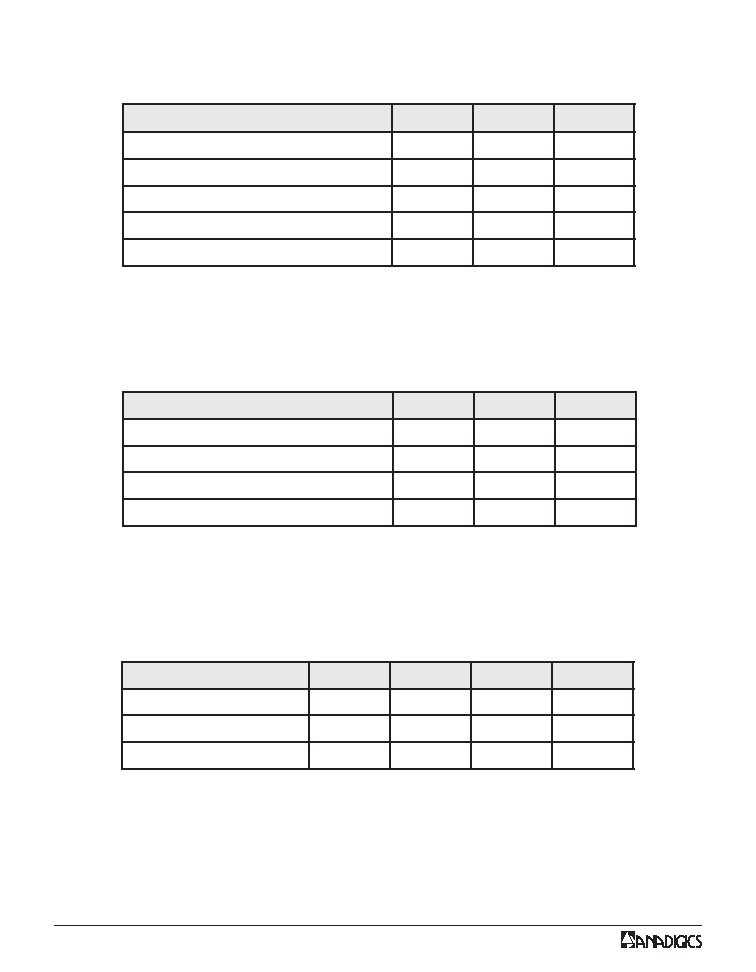
ELECTRICAL CHARACTERISTICS
Table 1: Absolute Minimum and Maximum Ratings
Exceeding the absolute maximum ratings can cause permanent damage to the de-
vice. These are absolute stress ratings only. Functional operation of the device is not
implied at these or any other conditions in excess of those given in the operations
sections of this data sheet. Exposure to maximum ratings for extended periods can
adversely affect device reliability.
Table 2: ESD Ratings
Although protection circuitry has been designed into this device, proper precau-
tions should be taken to avoid exposure to electrostatic discharge (ESD) during
handling and mounting. Human body model HBM employed is resistance = 1500
,
capacitance = 100pF.
Table 3: Logic Level Definitions
(V
CC
= 3.0 to 4.8 V, T
C
= 25 ± 3 ∞C)
R
E
T
E
M
A
R
A
P
N
I
M
X
A
M
T
I
N
U
(
e
g
a
tl
o
V
y
l
p
p
u
S
V
C
C
)
-
7
+
V
(
r
e
w
o
P
t
u
p
n
I
F
R
N
I
)
-
1
1
+
m
B
d
V
(
e
g
a
tl
o
V
l
o
r
t
n
o
C
r
e
w
o
P
P
M
A
R
)
-
8
.
1
V
(
e
r
u
t
a
r
e
p
m
e
T
e
g
a
r
o
t
S
T
G
T
S
)
5
5
-
0
5
1
C
∞
e
r
u
t
a
r
e
p
m
e
T
w
o
lf
e
R
m
u
m
i
x
a
M
-
0
4
2
C
∞
R
E
T
E
M
A
R
A
P
D
O
H
T
E
M
G
N
I
T
A
R
T
I
N
U
)
t
r
o
P
a
n
n
e
t
n
A
(
e
g
a
tl
o
V
d
l
o
h
s
e
r
h
T
D
S
E
M
B
H
5
1
V
k
)
s
t
u
p
n
I
l
o
r
t
n
o
C
(
e
g
a
tl
o
V
d
l
o
h
s
e
r
h
T
D
S
E
M
B
H
1
V
k
)
s
t
u
p
n
I
F
R
(
e
g
a
tl
o
V
d
l
o
h
s
e
r
h
T
D
S
E
M
B
H
1
V
k
)
s
t
r
o
P
X
R
(
e
g
a
tl
o
V
d
l
o
h
s
e
r
h
T
D
S
E
M
B
H
0
0
3
V
R
E
T
E
M
A
R
A
P
N
I
M
P
Y
T
X
A
M
T
I
N
U
H
O
V
2
.
1
-
3
V
L
O
V
2
.
0
-
-
5
.
0
V
t
n
e
r
r
u
C
s
a
i
B
t
u
p
n
I
-
-
0
1
mA

4
ADVANCED PRODUCT INFORMATION - Rev 0.3
02/2005
AWT6202
Table 7: Receiver Specifications
(Mode = RX (see control table), V
BATT
= 3.5 V, Z
IN
= Z
OUT
= 50
V
, ,
, ,
,
T
C
= 25 ± 3 ∞C)
Table 6: Operating Ranges
Parametric performance is guaranteed under specified operating conditions.
R
E
T
E
M
A
R
A
P
N
I
M
P
Y
T
X
A
M
T
I
N
U
S
T
N
E
M
M
O
C
(
e
g
a
tl
o
V
y
l
p
p
u
S
V
T
T
A
B
)
0
.
3
5
.
3
8
.
4
V
t
n
e
r
r
u
C
n
w
o
D
r
e
w
o
P
(
V
T
T
A
B
)
V
8
.
4
=
0
-
0
1
mA
V
(
t
n
e
r
r
u
C
X
R
T
T
A
B
)
V
8
.
4
=
0
-
0
3
mA
V
(
e
g
a
tl
o
V
l
o
r
t
n
o
C
P
M
A
R
)
2
.
0
-
6
.
1
V
V
P
M
A
R
e
c
n
a
ti
c
a
p
a
C
t
u
p
n
I
-
3
-
F
p
T
(
e
r
u
t
a
r
e
p
m
e
T
e
s
a
C
C
)
0
2
-
-
5
8
C
∞
e
l
c
y
C
y
t
u
D
-
-
0
5
%
R
E
T
E
M
A
R
A
P
N
I
M
P
Y
T
X
A
M
T
I
N
U
s
t
n
e
m
m
o
C
0
0
9
/
0
5
8
M
S
G
s
s
o
l
n
o
it
r
e
s
n
I
-
0
.
1
-
B
d
F
N
I
V
,
z
H
M
0
6
9
o
t
9
6
8
=
T
T
A
B
,
V
8
.
4
o
t
0
.
3
=
T
C
C
∞
5
8
+
o
t
0
2
-
=
S
C
P
/
S
C
D
s
s
o
l
n
o
it
r
e
s
n
I
-
2
.
1
-
B
d
F
N
I
H
M
0
9
9
1
o
t
5
0
8
1
=
,
z
V
T
T
A
B
,
V
8
.
4
o
t
0
.
3
=
T
C
C
∞
5
8
+
o
t
0
2
-
=
s
s
o
l
n
r
u
t
e
R
r
e
v
i
e
c
e
R
5
1
-
-
B
d
F
N
I
z
H
M
0
6
9
o
t
9
6
8
=
5
1
-
-
B
d
F
N
I
z
H
M
0
9
9
1
o
t
5
0
8
1
=
n
o
it
a
l
o
s
I
r
e
v
i
e
c
e
R
F
F
O
_
X
R
o
t
T
N
A
5
2
-
-
B
d
F
N
I
z
H
M
0
6
9
o
t
9
6
8
=
5
2
-
-
B
d
F
N
I
z
H
M
0
9
9
1
o
t
5
0
8
1
=
s
t
r
o
p
X
R
t
a
r
e
w
o
P
X
T
-
0
1
-
-
m
B
d
P
0
0
9
/
0
5
8
M
S
G
T
U
O
m
B
d
2
.
3
3
=
-
3
1
-
-
m
B
d
P
S
C
P
/
S
C
D
T
U
O
m
B
d
3
.
0
3
=

