03/2004
AWT6252
IMT/WCDMA 3.4V/27.5dBm
Linear Power Amplifier Module
PRELIMINARY DATA SHEET - Rev 1.3
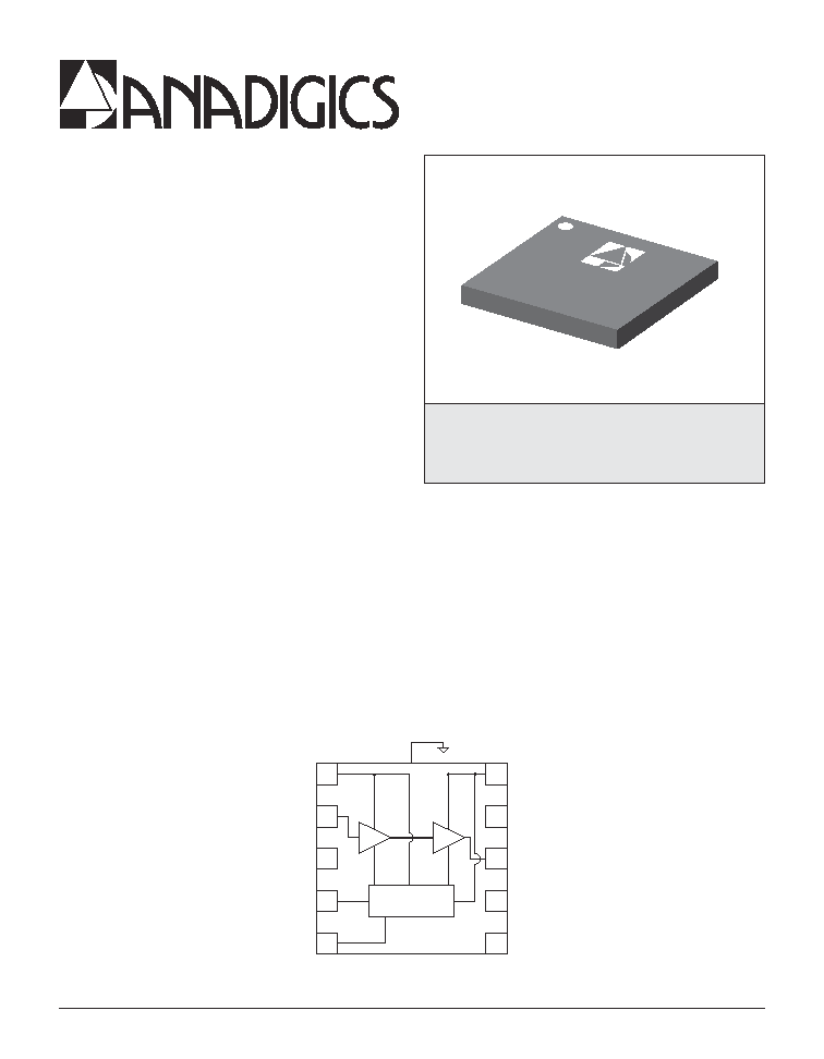
M7 Package
10 Pin 4 x 4 x 1.5 mm
Surface Mount Module
Figure 1: Block Diagram
Selectable bias modes that optimize efficiency for
different output power levels, and a shutdown mode
with low leakage current, increase handset talk and
standby time. The self-contained 4 x 4 x 1.5 mm surface
mount package incorporates matching networks
optimized for output power, efficiency, and linearity in a
50
system.
FEATURES
∑
InGaP HBT Technology
∑
High Efficiency: 39%
∑
Low Quiescent Current: 50 mA
∑
Low Leakage Current in Shutdown Mode: <1
µ
A
∑
V
REF
= +2.85 V (+2.75 V min over temp)
∑
Optimized for a 50
System
∑
Low Profile Miniature Surface Mount Package:
1.56mm Max
APPLICATIONS
∑
Dual Mode 3GPP Wireless Handsets
PRODUCT DESCRIPTION
The AWT6252 meets the increasing demands for
higher output power in 3GPP 1XRTT handsets. The PA
module is optimized for V
REF
= +2.85 V, a requirement
for compatibility with the QualcommÆ 6250 chipset.
The device is manufactured on an advanced InGaP
HBT MMIC technology offering state-of-the-art
reliability, temperature stability, and ruggedness.
AWT6252
Bias Control
V
CC
V
REF
RF
IN
RF
OUT
GND
V
MODE
1
7
5
8
10
6
GND at slug (pad)
3
9
4
2
GND
V
CC
GND
GND

2
PRELIMINARY DATA SHEET - Rev 1.3
03/2004
AWT6252
V
CC
RF
OUT
V
REF
RF
IN
V
MODE
GND
1
GND
10
2
3
4
5
6
9
8
7
V
CC
GND
GND
GND
GND
Figure 2: Pinout (X-ray Top View)
Table 1: Pin Description
N
I
P
E
M
A
N
N
O
I
T
P
I
R
C
S
E
D
1
V
C
C
e
g
a
tl
o
V
y
l
p
p
u
S
2
F
R
N
I
t
u
p
n
I
F
R
3
D
N
G
d
n
u
o
r
G
4
V
E
D
O
M
e
g
a
tl
o
V
l
o
r
t
n
o
C
e
d
o
M
5
V
F
E
R
e
g
a
tl
o
V
e
c
n
e
r
e
f
e
R
6
D
N
G
d
n
u
o
r
G
7
D
N
G
d
n
u
o
r
G
8
F
R
T
U
O
t
u
p
t
u
O
F
R
9
D
N
G
d
n
u
o
r
G
0
1
V
C
C
e
g
a
tl
o
V
y
l
p
p
u
S
PRELIMINARY DATA SHEET - Rev 1.3
03/2004
AWT6252
3
ELECTRICAL CHARACTERISTICS
Table 2: Absolute Minimum and Maximum Ratings
Stresses in excess of the absolute ratings may cause permanent
damage. Functional operation is not implied under these conditions.
Exposure to absolute ratings for extended periods of time may
adversely affect reliability.
Table 3: Operating Ranges
The device may be operated safely over these conditions; however, parametric performance is guaranteed
only over the conditions defined in the electrical specifications.
R
E
T
E
M
A
R
A
P
N
I
M
X
A
M
T
I
N
U
V
(
e
g
a
tl
o
V
y
l
p
p
u
S
C
C
)
0
5
+
V
V
(
e
g
a
tl
o
V
l
o
r
t
n
o
C
e
d
o
M
E
D
O
M
)
0
5
.
3
+
V
V
(
e
g
a
tl
o
V
e
c
n
e
r
e
f
e
R
F
E
R
)
0
5
.
3
+
V
P
(
r
e
w
o
P
t
u
p
n
I
F
R
N
I
)
-
0
1
+
m
B
d
T
(
e
r
u
t
a
r
e
p
m
e
T
e
g
a
r
o
t
S
G
T
S
)
0
4
-
0
5
1
+
C
∞
Notes:
(1) For operation at T
C
= +90
o
C and V
CC
= +3.2 V, P
OUT
is derated by 0.5 dB.
R
E
T
E
M
A
R
A
P
N
I
M
P
Y
T
X
A
M
T
I
N
U
S
T
N
E
M
M
O
C
)
f
(
y
c
n
e
u
q
e
r
F
g
n
it
a
r
e
p
O
0
2
9
1
-
0
8
9
1
z
H
M
V
(
e
g
a
tl
o
V
y
l
p
p
u
S
C
C
)
2
.
3
+
4
.
3
+
2
.
4
+
V
V
(
e
g
a
tl
o
V
e
c
n
e
r
e
f
e
R
F
E
R
)
5
7
.
2
+
0
5
8
.
2
+
-
5
9
.
2
+
5
.
0
+
V
"
n
o
"
A
P
"
n
w
o
d
t
u
h
s
"
A
P
V
(
e
g
a
tl
o
V
l
o
r
t
n
o
C
e
d
o
M
E
D
O
M
)
5
.
2
+
0
8
.
2
+
-
1
.
3
+
5
.
0
+
V
e
d
o
M
s
a
i
B
w
o
L
e
d
o
M
s
a
i
B
h
g
i
H
P
(
r
e
w
o
P
t
u
p
t
u
O
F
R
T
U
O
)
0
.
7
2
+
)
1
(
5
.
7
2
+
-
m
B
d
T
(
e
r
u
t
a
r
e
p
m
e
T
e
s
a
C
C
)
0
1
-
-
0
9
+
C
∞

4
PRELIMINARY DATA SHEET - Rev 1.3
03/2004
AWT6252
Table 4: Electrical Specifications
(T
C
= +25 ∞C, V
CC
= +3.4 V, V
REF
= +2.85 V, 50
system)
Notes:
(1) ACLR and Efficiency measured at 1950 MHz.
R
E
T
E
M
A
R
A
P
N
I
M
P
Y
T
X
A
M
T
I
N
U
S
T
N
E
M
M
O
C
n
i
a
G
5
.
4
2
2
2
7
1
5
.
6
2
5
.
4
2
5
.
0
2
9
2
7
2
4
2
B
d
P
T
U
O
V
,
m
B
d
5
.
7
2
+
=
E
D
O
M
V
0
=
P
T
U
O
V
,
m
B
d
6
1
+
=
E
D
O
M
V
5
8
.
2
+
=
P
T
U
O
V
,
m
B
d
6
1
+
=
C
C
,
V
5
.
1
=
V
E
D
O
M
V
5
8
.
2
+
=
t
e
s
ff
o
z
H
M
5
t
a
1
R
L
C
A
)
1
(
-
-
-
3
4
-
1
4
-
6
4
-
8
3
-
8
3
-
8
3
-
c
B
d
P
T
U
O
V
,
m
B
d
5
.
7
2
+
=
E
D
O
M
V
0
=
P
T
U
O
V
,
m
B
d
6
1
+
=
E
D
O
M
V
5
8
.
2
+
=
P
T
U
O
V
,
m
B
d
6
1
+
=
C
C
,
V
5
.
1
=
V
E
D
O
M
V
5
8
.
2
+
=
t
e
s
ff
o
z
H
M
0
1
t
a
2
R
L
C
A
-
-
-
0
6
-
2
6
-
0
6
-
0
5
-
0
5
-
8
4
-
c
B
d
P
T
U
O
V
,
m
B
d
5
.
7
2
+
=
E
D
O
M
V
0
=
P
T
U
O
V
,
m
B
d
6
1
+
=
E
D
O
M
V
5
8
.
2
+
=
P
T
U
O
V
,
m
B
d
6
1
+
=
C
C
,
V
5
.
1
=
V
E
D
O
M
V
5
8
.
2
+
=
y
c
n
e
i
c
if
f
E
d
e
d
d
A
-
r
e
w
o
P
)
1
(
7
3
5
.
8
9
1
9
3
5
.
9
5
.
1
2
-
-
-
%
P
T
U
O
V
,
m
B
d
5
.
7
2
+
=
E
D
O
M
V
0
=
P
T
U
O
V
,
m
B
d
6
1
+
=
E
D
O
M
V
5
8
.
2
+
=
P
T
U
O
V
,
m
B
d
6
1
+
=
C
C
,
V
5
.
1
=
V
E
D
O
M
V
5
8
.
2
+
=
)
q
c
I
(
t
n
e
r
r
u
C
t
n
e
c
s
e
i
u
Q
-
3
5
5
6
A
m
V
E
D
O
M
V
5
8
.
2
+
=
t
n
e
r
r
u
C
e
c
n
e
r
e
f
e
R
-
8
.
3
5
A
m
V
h
g
u
o
r
h
t
F
E
R
n
i
p
t
n
e
r
r
u
C
l
o
r
t
n
o
C
e
d
o
M
-
3
.
0
5
.
0
A
m
V
h
g
u
o
r
h
t
E
D
O
M
V
,
n
i
p
E
D
O
M
V
5
8
.
2
+
=
t
n
e
r
r
u
C
e
g
a
k
a
e
L
-
1
<
5
A
µ
V
C
C
V
,
V
2
.
4
+
=
F
E
R
,
V
0
=
V
E
D
O
M
V
0
=
d
n
a
B
e
v
i
e
c
e
R
n
i
e
s
i
o
N
-
9
3
1
-
7
3
1
-
z
H
/
m
B
d
z
H
M
0
7
1
2
o
t
z
H
M
0
1
1
2
s
c
i
n
o
m
r
a
H
o
f
2
o
f
4
,
o
f
3
-
-
5
4
-
0
5
-
0
3
-
0
3
-
c
B
d
e
c
n
a
d
e
p
m
I
t
u
p
n
I
-
-
1
:
2
R
W
S
V
l
e
v
e
L
t
u
p
t
u
O
s
u
o
ir
u
p
S
)
s
t
u
p
t
u
o
s
u
o
ir
u
p
s
ll
a
(
-
-
0
7
-
c
B
d
P
T
U
O
<
m
B
d
5
.
7
2
+
1
:
5
<
R
W
S
V
d
a
o
l
d
n
a
b
-
n
I
1
:
0
1
<
R
W
S
V
d
a
o
l
d
n
a
b
-
f
o
-
t
u
O
d
n
a
e
g
a
tl
o
v
ll
a
r
e
v
o
s
e
il
p
p
A
s
e
g
n
a
r
g
n
it
a
r
e
p
o
e
r
u
t
a
r
e
p
m
e
t
o
n
h
ti
w
s
s
e
r
t
s
h
c
t
a
m
s
i
m
d
a
o
L
e
r
u
li
a
f
r
o
n
o
it
a
d
a
r
g
e
d
t
n
e
n
a
m
r
e
p
1
:
8
-
-
R
W
S
V
V
C
C
P
,
V
0
.
5
+
=
N
I
m
B
d
5
+
=
g
n
it
a
r
e
p
o
ll
u
f
r
e
v
o
s
e
il
p
p
A
e
g
n
a
r
e
r
u
t
a
r
e
p
m
e
t

PRELIMINARY DATA SHEET - Rev 1.3
03/2004
AWT6252
5
APPLICATION INFORMATION
To ensure proper performance, refer to all related
Application Notes on the ANADIGICS web site:
http://www.anadigics.com
Shutdown Mode
The power amplifier may be placed in a shutdown
mode by applying logic low levels (see Operating
Ranges table) to both the V
REF
and V
MODE
voltages.
Table 5: Bias Control
Bias Modes
The power amplifier may be placed in either a Low
Bias mode or a High Bias mode by applying the
appropriate logic level (see Operating Ranges table)
to the V
MODE
voltage. The Bias Control table lists the
recommended modes of operation for various
applications.
C3
0.01µF
C4
2.2µF ceramic
GND
at slug
RF IN
2
9
1
6
7
10
8
5
4
3
V
CC
V
MODE
GND
RF
IN
GND
V
CC
GND
V
REF
GND
RF
OUT
VCC2
C1
0.01µF
VCC1
VMODE
VREF
C2
0.01µF
RF OUT
Figure 3: Application Circuit Schematic
N
O
I
T
A
C
I
L
P
P
A
P
T
U
O
S
L
E
V
E
L
S
A
I
B
E
D
O
M
V
F
E
R
V
E
D
O
M
V
C
C
r
e
w
o
p
w
o
l
-
A
M
D
C
<
m
B
d
6
1
+
w
o
L
V
5
8
.
2
+
V
5
8
.
2
+
>
5
.
1
+
r
e
w
o
p
h
g
i
h
-
A
M
D
C
m
B
d
6
1
+
>
h
g
i
H
V
5
8
.
2
+
V
0
4
.
3
+
n
w
o
d
t
u
h
S
-
n
w
o
d
t
u
h
S
V
0
V
0
-

6
PRELIMINARY DATA SHEET - Rev 1.3
03/2004
AWT6252
PACKAGE OUTLINE
Figure 4: M7 Package Outline - 10 Pin 4 x 4 x 1.5 mm Surface Mount Module
Figure 5: Branding Specification
5
5

PRELIMINARY DATA SHEET - Rev 1.3
03/2004
AWT6252
7
COMPONENT PACKAGING
E
P
Y
T
E
G
A
K
C
A
P
H
T
D
I
W
E
P
A
T
H
C
T
I
P
T
E
K
C
O
P
Y
T
I
C
A
P
A
C
L
E
E
R
A
I
D
L
E
E
R
X
A
M
m
m
5
.
1
x
4
X
4
m
m
2
1
m
m
8
0
0
5
2
"
3
1
Figure 6: Tape & Reel Packaging
Table 6: Tape & Reel Dimensions
WARNING
ANADIGICS products are not intended for use in life support appliances, devices or systems. Use of an ANADIGICS
product in any such application without written consent is prohibited.
IMPORTANT NOTICE
ANADIGICS, Inc.
141 Mount Bethel Road
Warren, New Jersey 07059, U.S.A.
Tel: +1 (908) 668-5000
Fax: +1 (908) 668-5132
URL: http://www.anadigics.com
E-mail: Mktg@anadigics.com
ANADIGICS, Inc. reserves the right to make changes to its products or to discontinue any product at any time without
notice. The product specifications contained in Advanced Product Information sheets and Preliminary Data Sheets are
subject to change prior to a product's formal introduction. Information in Data Sheets have been carefully checked and are
assumed to be reliable; however, ANADIGICS assumes no responsibilities for inaccuracies. ANADIGICS strongly urges
customers to verify that the information they are using is current before placing orders.
PRELIMINARY DATA SHEET - Rev 1.3
03/2004
8
AWT6252
ORDERING INFORMATION
R
E
B
M
U
N
R
E
D
R
O
E
R
U
T
A
R
E
P
M
E
T
E
G
N
A
R
E
G
A
K
C
A
P
N
O
I
T
P
I
R
C
S
E
D
G
N
I
G
A
K
C
A
P
T
N
E
N
O
P
M
O
C
8
P
7
M
2
5
2
6
T
W
A
0
1
-
o
0
9
+
o
t
C
o
C
n
i
P
0
1
m
m
5
.
1
x
4
x
4
t
n
u
o
M
e
c
a
f
r
u
S
e
l
u
d
o
M
l
e
e
R
r
e
p
s
e
c
e
i
p
0
0
5
2
,l
e
e
R
d
n
a
e
p
a
T