
AWT921S11
Integrated High Power Amp 900 MHz
Advanced Product information
Rev. 6
DESCRIPTION
The AWT921 is a monolithic amplifier for use in
communication systems that require high gain and output
intercept point. This device has been specifically designed
for multi carrier and micro cell base station applications.
FEATURES
l
High output power levels
l
High Efficiency
l
True Surface Mount Package with Integrated Heat Slug
l
Internal Bias Circuit Requiring Nominal Input Voltages
+10%
l
Low Cost
l
Off Chip Output Matching Circuit Allows Application
Optimization
ABSOLUTE MAXIMUM RATINGS
PIN
SIGNAL
MAX RATING
PIN
SIGNAL
MAX RATING
2
V
DD
+7V
DC
11
V
REF
+7
V
DC
3
RF
IN
+20
dBm
12
V
SS
-7
V
DC
4,5
V
D1
+10
V
DC
18,19,20,21,22,23,24,25
V
D3
+10
V
DC
8,9
V
D2
+10
V
DC
Operating Temperature: -30 to + 85
o
C
Storage Temperature: -55 to + 100
o
C
S11
SSOP-28 Wide Body
28 Pin Wide Body w/ Heat Slug
A

2
A
AWT921S11
Advanced Product Information - Rev. 6
ELECTRICAL SPECIFICATIONS:
(1)
(Pin +12 dBm, fo = 925-960 MHz, V
DS1
= V
DS2
= V
DS3
= 8.5V, V
SS
= - 3V,V
REF
=+5V,V
DD
=+5V,Tc=25C, 50W System
(2)
PARAMETER
SYMBOL
MIN
TYP
MAX
UNITS
Frequency
fo
925
-
960
MHz
Power
Output
P
OUT
-
+
39
-
dBm
Power Added Efficiency
Eff
-
40
-
%
Gain
@
P
OUT
= +39 dBm
@
P
OUT
= +30 dBm
PG
-
29
30
-
dB
Harmonics
(3)
2nd
3rd
4th
-
-
37
47
50
-
dBc
Stability: - 60 dBc all spurious outputs
relative
to desired signal
-
-
3:1
-
VSWR load, all
phase angles
Bias supply currents
I
SS
I
REF
I
DD
-
8
1.2
8
-
mA
mA
mA
Quiescent Currents
I
DQ1
I
DQ2
I
DQ3
-
100
250
200
-
mA
mA
mA
Input Return Loss
10
-
-
dB
Gain Flatness vs. Frequency
@ Pout = +39 dBm
@ Pout = +30 dBm
PG
�
0.5
�
0.5
-
-
dB
dB
Thermal Resistance
4
-
-
4.5
-
C/W
NOTES:
1: As measured in ANADIGICS test fixture, see application section
2: 50W Measurement system after off chip matching circuit, input terminated in 50W
3: Measured at Pout =+ 39 dBm
4: Thermal resistance for junction to bottom of slug. Qjc= (Tj-Tc)/((I
D1
+I
D2
+I
D3
)*V
SUP
- P
OUT
)
CHARACTERIZATION DATA
(1)
-
Conditions unless otherwise stated (Pin +12 dBm, fo = 925-960 MHz, V
DS1
= V
DS2
= V
DS3
= 8.5V,
V
SS
= - 3V, V
REF
= +5V, V
DD
=+ 5 V, Tc=25�C, 50 W system
(2)
)
30
32
34
36
38
40
P
out (dB
m
)
0
10
20
30
40
50
60
70
80
90
100
P
add E
ff (%
)
0
2
4
6
8
10 12 14
Pin (dBm)
Pout
Eff
Pout & Eff vs. Pin
35
36
37
38
39
40
41
42
43
Pout
(dBm
)
0
10
20
30
40
50
60
Padd Ef
f
(%
)
920
930
940
950
960
Freq (MHz)
Pout
Eff
Pout & Eff vs. Frequency

3
A
AWT921S11
Advanced Product Information - Rev. 6
ADC
90
95
100
105
110
115
120
Bia
s Ckt Cu
r
r
e
n
t
G
a
in
2
3
4
5
6
7
8
Vref (Volts)
Bias Ckt Gain vs Vref
Idq3/Iref
100
150
200
250
300
350
400
I
q3 (
m
A)
1
1.05
1.1
1.15
1.2
1.25
1.3
Ire
f
(mA
)
-40 -20 0 20 40 60 80 100
Temperature (C)
Iq3
Iref
Iq3 & Iref vs Temperature
35
36
37
38
39
40
41
P
out (dB
m
)
5
6
7
8
9
10
11
Vsup (V)
Pout
Pout vs. Supply Voltage
0
20
40
60
80
100
120
Idq3 (mA
)
0
2
4
6
8
Vdd (Volts)
Idq3 vs Vdd
0
100
200
300
400
500
600
I
dq3
(
m
A
)
0
2
4
6
8
Vref (Volts)
Rref=1.5 K
Rref=3 K
Rref=6 K
Idq3 vs Vref
100
150
200
250
300
350
400
450
500
Idq3 (mA
)
-7
-6
-5
-4
-3
-2
Vss (Volts)
Idq3 vs Vss
Notes:
1: As measured in ANADIGICS test fixture, see application section
2: 50W Measurement system after off chip matching circuit, input terminated in 50W
CHARACTERIZATION DATA:
(1)
Conditions unless otherwise stated (Pin +12 dBm, fo = 925-960 MHz,
V
DS1
= V
DS2
= V
DS3
= 8.5V, V
SS
= - 3V, V
REF
= + 5V, V
DD
=+ 5V, Tc=25
O
C, 50W system)
(2)
ADC
AWT921S11
ADC
4
A
AWT921S11
Advanced Product Information - Rev. 6
32
33
34
35
36
37
38
39
40
Pout (
d
Bm)
& SS G
a
in (
d
B)
33
35
37
39
41
43
Eff (
%
)
-40 -20 0 20 40 60 80 100
Temperature (C)
Pout
Eff
SS PG
Pout,PG,& Eff vs Temperature
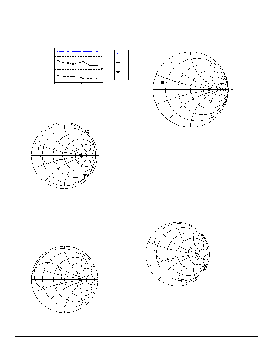
Load + 3.7 + 3.9 j
Output Load Impedance as seen
by the device
M A R K E R 1
0 . 9 5 7 5 0 0 0 0 0 G H z
M A R K E R T O M A X
M A R K E R T O M I N
M A R K E R R E A D O U T
F U N C T I O N S
0
. 2
. 5
1
2
5
. 2
- . 2
. 5
- . 5
1
- 1
2
- 2
5
- 5
0 . 0 5 0 0 0 0 0 0 0 - 2 . 8 0 0 0 0 0 0 0 0 G H z
S 1 1 R E V E R S E R E F L E C T I O N
I M P E D A N C E
C H 4 - S 1 1
R E F E R E N C E P L A N E
9 . 0 8 2 1 c m
0 . 0 9 8 1 2 5 0 0 0 G H z
1 . 9 2 0 0 0 0 0 0 0 G H z
2 . 8 0 0 0 0 0 0 0 0 G H z
7 . 0 7 4
3 6 . 9 1 9
1 1 . 4 4 6
3 . 1 3 3
1 3 1 . 9 0 6 j
- 1 3 . 5 0 1 j
- 1 1 1 . 6 4 1 j
- 2 4 . 5 5 0 j
2
3
4
1
2
3
4
M A R K E R 1
0 . 9 5 7 5 0 0 0 0 0 G H z
M A R K E R T O M A X
M A R K E R T O M I N
M A R K E R R E A D O U T
F U N C T I O N S
0
. 2
. 5
1
2
5
. 2
- . 2
. 5
- . 5
1
- 1
2
- 2
5
- 5
0 . 0 5 0 0 0 0 0 0 0 - 2 . 8 0 0 0 0 0 0 0 0 G H z
S 1 1 R E V E R S E R E F L E C T I O N
I M P E D A N C E
C H 4 - S 1 1
R E F E R E N C E P L A N E
9 . 0 8 2 1 c m
0 . 0 9 8 1 2 5 0 0 0 G H z
1 . 9 2 0 0 0 0 0 0 0 G H z
2 . 8 0 0 0 0 0 0 0 0 G H z
7 . 6 5 9
3 7 . 2 3 7
1 3 . 3 0 8
4 . 4 6 6
1 6 1 . 1 8 1 j
- 1 1 . 8 1 7 j
- 1 7 1 . 1 2 6 j
- 6 0 . 0 4 4 j
2
3
4
1
2
3
4
S A V E M E M O R Y
T O H A R D D I S K
S A V E M E M O R Y
T O F L O P P Y D I S K
R E C A L L M E M O R Y
F R O M H A R D D I S K
R E C A L L M E M 0 O R Y
F R O M F L O P P Y D I S K
P R E S S < E N T E R >
T O S E L E C T
0
. 2
. 5
1
2
5
. 2
- . 2
. 5
- . 5
1
- 1
2
- 2
5
- 5
0 . 0 5 0 0 0 0 0 0 0 - 2 . 8 0 0 0 0 0 0 0 0 G H z
S 2 2 R E V E R S E R E F L E C T I O N
I M P E D A N C E
T R A C E M E M O R Y
D I S K O P E R A T I O N S
C H A N N E L 4
1
3
4
Output Impedance as seen by V
DS3
Impedance as seen V
DS2
Impedance as seen by V
DS1

5
ANADIGICS, Inc.
35 Technology Drive
Warren, New Jersey 07059
Tel: (908) 668-5000 / Fax: (908) 668-5132
Email: Mkg@anadigics.com
www.anadigics.com
IMPORTANT NOTICE
ANADIGICS, Inc. reserves the right to make changes to its products or discontinue any product at any time without notice. The Advanced Product data
sheets and product specifications contained in this data sheet are subject to change prior to a products formal introduction. The information in this data
sheet has been carefully checked and is assumed to be reliable. However, ANADIGICS assumes no responsibility for inaccuracies. ANADIGICS strongly
urges customers to verify that the information they are using is current before placing orders.
WARNING
ANADIGICS products are not intended for use in life support appliances, device, or systems. Use of an ANADIGICS product in any such application
without written consent is prohibited.
A
AWT921S11
Advanced Product Information - Rev. 6
D
T
H E A T S I N K
E
S
A
A
2
A
1
h
a
S L U G
L E
C
L
e
PACKAGE OUTLINE DRAWING
INCHES
MILLIMETERS
SYMBOL
MIN.
MAX.
MIN.
MAX.
NOTE
A
0.087
0.093
2.21
2.36
A
1
0.000
0.004
0.00
0.10
A
2
0.087
0.089
2.21
2.25
B
0.008
0.012
0.36
0.46
C
0.007
0.009
0.18
0.25
D
0.400
0.408
10.16
10.36
2
E
0.292
0.296
7.42
7.52
2
e
0.025
BSC
0.64
BSC
4
H
0.410
0.418
10.41
40.62
h
0.018
0.024
0.48
0.61
L
0.034
0.038
0.86
0.97
LE
0.84
1.37
a
0
8
0
8
S
0.139
0.141
3.54
3.55
5
T
0.349
0.351
8.86
8.92
5
Notes
:
1. Controlling dimensions : inches.
2. Dimension d does not include mold flash, protrusions
or gate burrs. Mold flash, protrusions and gate burrs
shall not exceed 0.006 (0.16mm).
3. Dimension e does not include inter-lead or protrusions.
Inter-lead flash and protrusions shall not exceed 0.010
(0.25mm) per side.
4. Maximum lead twist/skew to be 0.002 (0.05mm).
5. Mold flash shall not extend more than 0.010 (0.25mm)
on any edge of heat slug.
ADC