05/2003
RFS1003
5.1-5.9 GHz U-NII Power Amplifier
Applications
∑
U-NII fixed-wireless CPE
∑
5 GHz ISM band wireless equipment
∑
WLAN/802.11a/HIPERLAN/2
1
2
3
4
5
6
19
20
21
22
23
24
18
17
16
15
14
13
12
11
10
9
8
7
N/
C
GN
D
VD
1
GN
D
VD
2
GN
D
N/C
GND
RF OUT
RF OUT
RF OUT
GND
VG
3
GN
D
VG
2
GN
D
VG
1
GN
D
N/C
GND
RF IN
GND
N/C
N/C
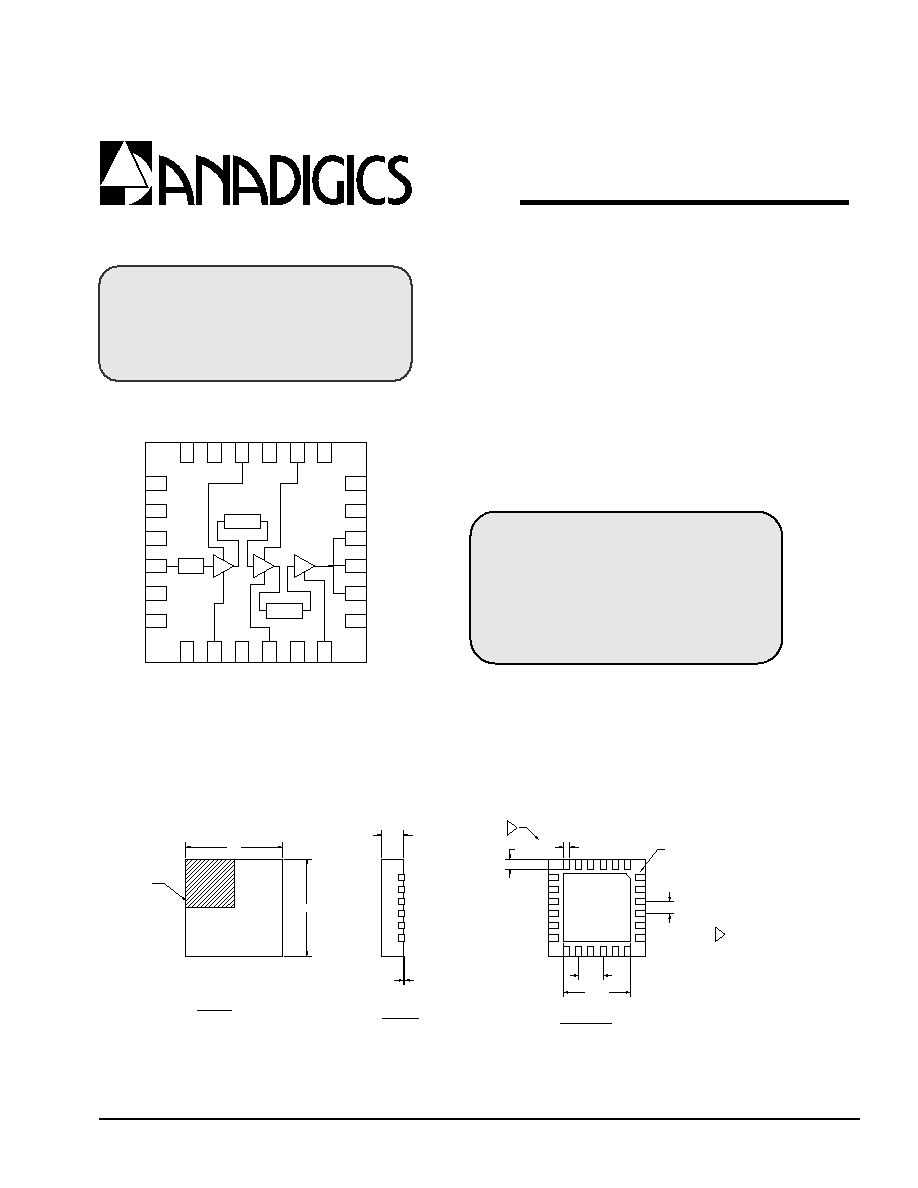
Interstage
Match
Interstage
Match
Input
Match
Functional Block Diagram
Product Description
The RFS1003 power amplifier is a high-power, high-
performance GaAs MESFET IC designed for use in
transmit applications in the 5.1-5.9 GHz frequency
band. With a P1dB of 29 dBm, the device is ideal as a
final stage for wireless applications requiring high
transmit linearity. The input of the PA is matched to 50
ohms and the output can be easily matched for optimum
linearity and power performance at the desired
frequency of operation between 5.1 and 5.9 GHz.
Product Features
∑
29 dBm P1dB@7V
∑
24 dBm P1dB@3V
∑
20 dB gain
∑
Input matched to 50 ohms
∑
Simple output matching
0.05
2.80 SQ
1.00
0.275
0.225
0.45
0.35
0.50 TYP
TOP VIEW
SIDE VIEW
BOTTOM VIEW
1
1 ALL DIMENSIONS ARE IN
MILLIMETERS, ANGLES IN DEGREES.
2 THE TERMINAL #1 IDENTIFIER AND
PAD NUMBERING CONVENTION SHALL
CONFORM TO JESD 95-1 SPP-012
3 LEAD COPLANARITY: 0.05 MAX.
4 DIMENSION APPLIES TO METALLIZED
PAD AND IS MEASURED BETWEEN 0.25
AND 0.30 MM FROM PAD TIP.
4
24
Pin 1
4.00
4.00
INDEX AREA
1.00
0.80
4x4 mm Package Outline

05/2003
2
RFS1003
5.1-5.9 GHz U-NII Power Amplifier
Specification
Parameter
1
Min.
Typ.
Max.
Unit
Condition
Overall
Frequency Range
5150
5850
MHz
Output P1dB
29
dBm
V
DD
= 7V
24
dBm
V
DD
= 3V
Efficiency at P1dB
28
%
Small Signal Gain
20
dB
P
IN
= -20 dBm; V
DD
= 7V
21
dB
P
IN
= -20 dBm; V
DD
= 3V
Gain Flatness
±0.5
dB
Across 100 MHz Band
Harmonics
2
nd
Harmonic
-35
dBc
3
rd
Harmonic
-35
dBc
Spurious (Stability)
2
-60
dBc/30 kHz
P
IN
= -30 to +10 dBm
Reverse Isolation
50
dB
Noise Figure
8.7
dB
Input Return Loss
10
15
dB
Output Return Loss
11
dB
Power Supply
Drain Operating Voltage
3
7
V
Gate Operating Voltage
-1.1
V
Current Consumption
400
mA
V
DD
= 7V
350
mA
V
DD
= 3V
Gate Leakage Current
25
µA
Note 1: Test Conditions: V
DD
= 7.0V, P
IN
= +10dBm, Freq. = 5850MHz, V
GG
= -1.1 V, T =25C.
Note 2: Load VSWR is set to 7:1 and the angle is varied 360 degrees.
Absolute Maximum Ratings
Parameter
Rating
Unit
DC Power Supply
8.0
V
DC Gate Voltage
-5.0 min, -0.5 max
V
DC Supply Current
1000
mA
Maximum RF input level
+13
dBm
Operating Ambient Temperature
-40 to +85
∞C
Storage Temperature
-55 to +150
∞C
Ordering Information
Part Number
PRFS-1003-0EVL
-40 to +85
Evaluation Board
1
PRFS-1003-0005
-40 to +85
13" Reverse Tape/Reel
2500 pcs.
PRFS-1003-0006
-40 to +85
13" Tape/Reel
2500 pcs.
PRFS-1003-0007
-40 to +85
7" Reverse Tape/Reel
1000 pcs.
PRFS-1003-0008
-40 to +85
7" Tape/Reel
1000 pcs.
PRFS-1003-0009
-40 to +85
Bulk ≠ 4x4 mm 24-pin LPCC
1-999 pcs.
Quantity
Package Description
Temp. Range ( ∞C)

3
05/2003
NOTES

05/2003
4
IMPORTANT NOTICE
ANADIGICS, Inc. reserves the right to make changes to its products or to discontinue any product at any time without notice.
The product
specifications contained in Advanced Product Information sheets and Preliminary Data Sheets are subject to change prior to a product's formal
introduction.
Information in Data Sheets have been carefully checked and are assumed to be reliable; however, ANADIGICS assumes no
responsibilities for inaccuracies. ANADIGICS strongly urges customers to verify that the information they are using is current before placing orders.
WARNING
ANADIGICS products are not intended for use in life support appliances, devices or systems. Use of an ANADIGICS product in any such application
without written consent is prohibited.
ANADIGICS, Inc.
141 Mount Bethel Road
Warren, New Jersey 07059,U.S.A.
Tel: +1(908)668-5000
Fax: +1(908)668-5132
URL: http://www.anadigics.com
E-mail: Mktg@anadigics.com