 | –≠–ª–µ–∫—Ç—Ä–æ–Ω–Ω—ã–π –∫–æ–º–ø–æ–Ω–µ–Ω—Ç: AN221E02 | –°–∫–∞—á–∞—Ç—å:  PDF PDF  ZIP ZIP |

DS030600-U002a
- 1 -
AN221E02 Datasheet
Entry Level, Dynamically Reconfigurable
FPAA With Enhanced I/O
www.anadigm.com

DS030600-U002a
- 2 -
Disclaimer
Anadigm reserves the right to make any changes without further notice to any products herein. Anadigm makes no
warranty, representation or guarantee regarding the suitability of its products for any particular purpose, nor does
Anadigm assume any liability arising out of the application or use of any product or circuit, and specifically disclaims
any and all liability, including with out limitation consequential or incidental damages. "Typical" parameters can and
do vary in different applications. All operating parameters, including "Typicals" must be validated for each customer
application by customer's technical experts. Anadigm does not in this document convey any license under its patent
rights nor the rights of others. Anadigm software and associated products cannot be used except strictly in
accordance with an Anadigm software license. The terms of the appropriate Anadigm software license shall prevail
over the above terms to the extent of any inconsistency.
© Anadigm
Æ
Ltd. 2003
© Anadigm
Æ
, Inc. 2003
All Rights Reserved.
AN221E02 Datasheet ≠ Entry Level, Dynamically Reconfigurable FPAA With Enhanced I/O
DS030600-U002a
- 3 -
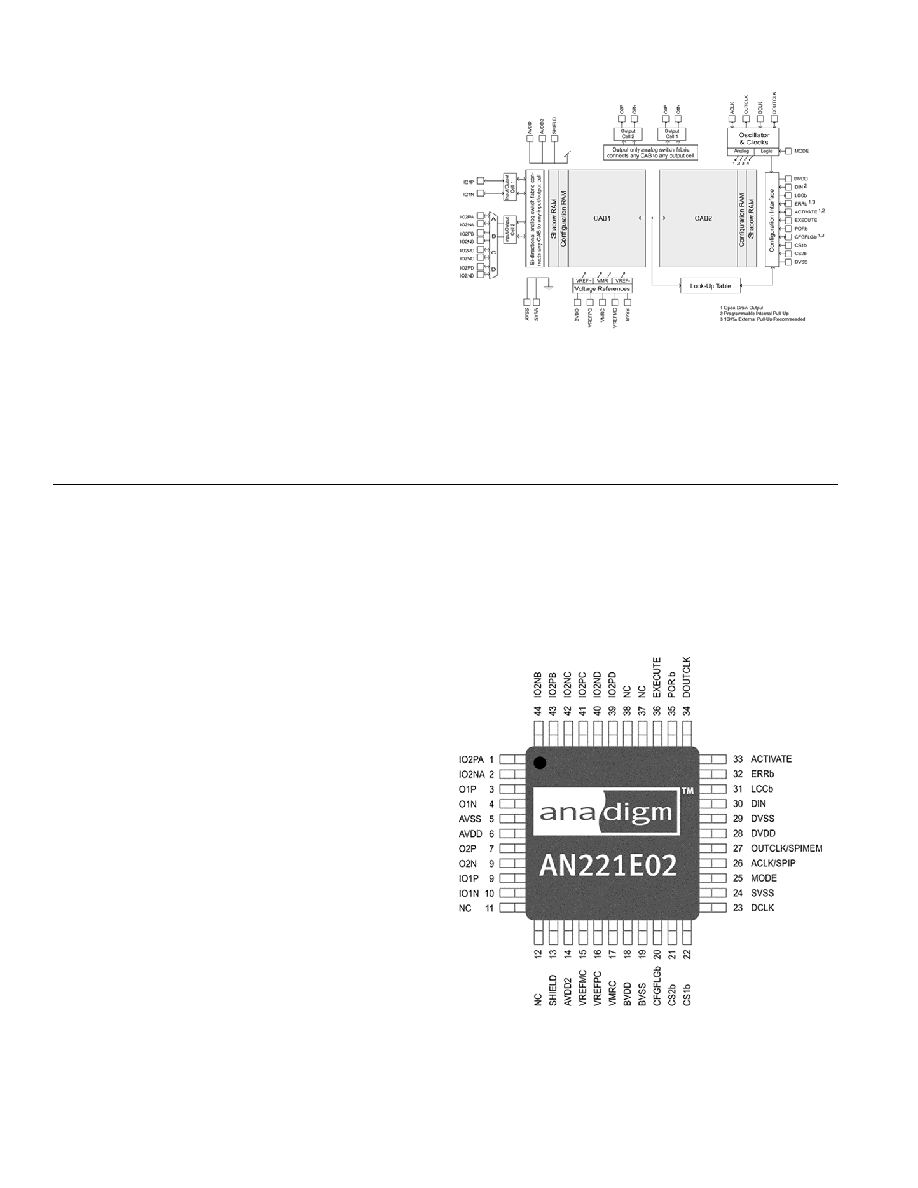
PRODUCT AND ARCHITECTURE OVERVIEW
The AN221E02 device is a low-cost, entry-level version of the
Anadigmvortex FPAA. The device consists of a two fully
Configurable Analog Blocks (CABs), surrounded by a fabric of
programmable interconnect resources. Each device has two
configurable I/Os and two dedicated outputs ≠ which allows for
maximum flexibility to the system designer.
These devices can be configured both in the static and in the
dynamic mode.
Using the on-chip LUT, these devices also accommodate
nonlinear functions such as sensor response linearization and
arbitrary waveform synthesis. In addition, the AN221E04 devices
allow designers to implement an integrated 8-bit analog-to-digital
converter on the FPAA, eliminating the potential need for an
external converter.
Packaged in a standard 44-pin TQFP package, these devices
maintain pin compatibility with the larger FPAA devices (i.e. the
AN221E04); allowing designers the ability to migrate up the
density curve
Figure 1: Architectural overview of the AN221E02 device
With dynamic reconfigurability, the functionality of the
AN221E02 can be reconfigured in-system by the designer or
on-the-fly by a microprocessor. A single AN221E02 can thus
be programmed to implement multiple analog functions
and/or to adapt on-the-fly to maintain precision operation
despite system degradation and aging.
PRODUCT FEATURES
∑
Two CABs, Two configurable I/O, two dedicated
outputs
∑
Static and Dynamic reconfiguration
∑
256 Byte Look-Up Table (LUT) for linearization and
arbitrary signal generation
∑
8-bit SAR analog≠to≠digital converter
∑
Fully differential architecture
o
SNR Broadband 80dB
o
SNR Narrowband (audio) 100dB
∑
Total Harmonic Distortion (THD): 80dB
∑
Fully differential I/O buffering with options for single ended
to differential conversion
∑
Low input offset through chopper stabilized amplifiers
o
DC offset <100µV
∑
4:1 Input multiplexer
∑
Typical Signal Bandwidth: DC-2MHz (Bandwidth is CAM
dependent)
∑
Package: 44-pin QFP (10x10x2mm)
o
Lead pitch 0.8mm
∑
Supply voltage: 5V
ORDERING CODES
AN221E02-QFPSP
Dynamically reconfigurable FPAA
Sample Pack
AN221E02-QFPTY
Dynamically reconfigurable FPAA
Tray (96 pcs)
AN221E02-QFPTR
Dynamically reconfigurable FPAA
Tape and Reel (1000 pcs)
AN221D04-EVAL
Anadigmvortex Evaluation Kit
APPLICATIONS
∑
Intelligent sensor modules
∑
Tunable filters
∑
Programmable analog front-end to DSPs
∑
Self-calibrating systems
∑
Compensation for aging of system components
∑
Dynamic recalibration of remote systems
∑
Ultra-low frequency signal conditioning
∑
Custom analog signal processing
[For more detailed information on the features of the AN221E02 device,
please refer to the Anadigmvortex Silicon User Manual coming soon.]

AN221E02 Datasheet ≠ Entry Level, Dynamically Reconfigurable FPAA With Enhanced I/O
DS030600-U002a
- 4 -
ELECTRICAL CHARACTERISTICS
Absolute Maximum Ratings
Parameter
Symbol
Min
Typ
Max
Unit
Comment
DC Power Supplies
AVDD(2)
BVDD
DVDD
-0.5
-
5.5 V
V
AVSS, BVSS, DVSS and SVSS all
held to 0.0 V
a
xVDD to xVDD Offset
-0.5
0.5
V
Ideally all supplies should be at the
same voltage
Package Power Dissipation
Pmax 25∞C
Pmax 85∞C
-
-
1.8
0.73
W
Still air, No heatsink, 4 layer board,
44 pins.
ja = 55∞C/W
Analog and Digital Input Voltage
Vinmax
Vss-0.5
-
Vdd+0.5
V
Ambient Operating Temperature
Top
-40
-
85
∞C
Storage Temperature
Tstg
-65
150
∞C
a
Absolute Maximum DC Power Supply Rating - The failure mode is non-catastrophic for Vdd of up to 7 volts, but will cause reduced
operating life time. The additional stress caused by higher local electric fields within the CMOS circuitry may induce metal migration,
oxide leakage and other time/quality related issues.
Recommended Operating Conditions
Parameter
Symbol
Min
Typ
Max
Unit
Comment
DC Power Supplies
AVDD(2)
BVDD
DVDD
4.75
5.00
5.25
V
AVSS, BVSS, DVSS and SVSS all
held to 0 V
Analog Input Voltage.
Vina
VMR-1.9
-
VMR+1.9
V
VMR is 2.0 volts above AVSS
Digital Input Voltage
Vind
0
-
DVDD
V
Junction Temp
Tj
-40
-
125
∞C
Assume a package
ja = 55∞C/W
b
b
In order to calculate the junction temperature you must first empirically determine the current draw (total Idd) for the design. Once the
current consumption established then the following formula can be used; Tj = Ta + Idd x Vdd x 55 ∞C/W, where Ta is the ambient
temperature. The worst case
ja of 55 ∞C/W assumes no air flow and no additional heatsink of any type.
General Digital I/O Characteristics (Vdd = 5v +/- 10%, -40 to 85 deg.C)
Parameter
Symbol
Min
Typ
Max
Unit
Comment
Input Voltage Low
Vih
0
-
30
-
% of DVDD
Input Voltage High
Vil
70
-
100
-
% of DVDD
Output Voltage Low
Vol
0
-
20
-
% of DVDD
Output Voltage High
Voh
80
-
100
-
% of DVDD
Input Leakage Current
Iil
-
-
±1.0
µA
All pins except DCLK
Input Leakage Current
Iil
-
±12.0
-
µA
DCLK if a crystal is connected and
the on-chip oscillator is used
Max. Capacitive Load
Cmax
-
-
10
pF
The maximum load for a digital
output is 10 pF // 10 Kohm
Min. Resistive Load
Rmin
10
-
-
Kohm
The maximum load for a digital
output is 10 pF // 10 Kohm
DCLK Frequency
Fmax
-
-
40
MHz
For MODE = 1, Max DCLK is
16 MHz
ACLK Frequency
Fmax
-
-
40
MHz
Divide down to <8 MHz prior to use
as a CAB clock
Clock Duty Cycle
-
45
-
55
%
All clocks

AN221E02 Datasheet ≠ Entry Level, Dynamically Reconfigurable FPAA With Enhanced I/O
DS030600-U002a
- 5 -
Detailed Digital I/O Interface Characteristics: Vdd = 5.0volts
LCCb
Parameter
Symbol
Min
Typ
Max
Unit
Comment
Output Voltage Low
Vol
Vss
-
150
mV
Load 20pF//50Kohm to Vss
Output Voltage High
Voh
4.5
-
Vdd
V
Load 20pF//50Kohm to Vss
Max. Capacitive Load
Cmax
-
-
20
pF
Maximum load 20 pF // 50 Kohm
Min. Resistive Load
Rmin
50
-
-
Kohm
Maximum load 20 pF // 50 Kohm
Current Sink
Isnkmax
-
-
15
mA
LCCb pin shorted to Vdd
Current Source
Isrcmax
-
-
4
mA
LCCb pin shorted to Vss
CFGFLG, ACTIVATE
Parameter
Symbol
Min
Typ
Max
Unit
Comment
Input Voltage Low
Vil
0
30
%
% of DVDD
Input Voltage High
Vih
70
100
%
% of DVDD
Output Voltage Low
Vol
Vss
-
85
mV
Pin load =
Internal pullup + 20pF//50K to Vss
Output Voltage High
Voh
4.5
-
Vdd
V
Pin load =
Internal pullup + 20pF//50K to Vss
Output Voltage Low
Vol
Vss
-
200
mV
Pin Load =
External 5K ohm pullup +
20pF//50K to Vss
Output Voltage High
Voh
4.5
-
Vdd
V
Pin Load =
External 5Kohm pullup +
20pF//50K to Vss
Max. Capacitive Load
Cmax
-
-
50
pF
Maximum load 50 pF // 50 Kohm
Min. Resistive Load
Rmin
50
-
-
Kohm
Maximum load 50 pF // 50 Kohm
Current Sink
Isnkmax
-
-
2.5
mA
Pin shorted to Vdd
Current Source
Isrcmax
-
-
200
µA
Pin shorted to Vss
External Resistive Pullup
Rpullupext
5
7.5
10
Kohm
Use only if internal pullup is
deselected
ERRb
Parameter
Symbol
Min
Typ
Max
Unit
Comment
Input Voltage Low
Vil
0
30
%
% of DVDD
Input Voltage High
Vih
70
100
%
% of DVDD
Output Voltage Low
Vol
Vss
-
50
mV
Output Voltage High
Voh
4.9
-
Vdd
V
Max. Capacitive Load
Cmax
-
-
50
pF
Maximum load 50 pF // 50 Kohm
Min. Resistive Load
Rmin
50
-
-
Kohm
Maximum load 50 pF // 50 Kohm
Current Sink
Isnkmax
-
-
10
mA
Current Source
Isrcmax
-
-
0
µA
External Resistive Pullup
Rpullupext
10
10
10
Kohm
DCLK,Mode,DIN,EXECUTE,PORb,CS1b,CS2b
Parameter
Symbol
Min
Typ
Max
Unit
Comment
Input Voltage Low
Vil
0
-
30
%
% of DVDD
Input Voltage High
Vih
70
-
100
%
% of DVDD