AAT2801
Multi-Mode Charge Pump for
White LED Backlight and Flash Applications
2801.2006.04.1.3
1
ChargePump
TM
General Description
The AAT2801 is a member of AnalogicTech's Total
Power Management ICTM (TPMICTM) product family.
It has a dual charge pump architecture designed to
support both the white LED backlight and flash appli-
cations for systems operating with Lithium-Ion bat-
teries. The backlight charge pump provides power
required to drive up to four LEDs. To maximize
power efficiency, it automatically selects 1X, 1.5X, or
2X mode. The device produces current levels up to
30mA on each of its four current source outputs.
AnalogicTech's Simple Serial ControlTM (S
2
CwireTM)
interface is used to enable, disable, and set the LED
drive current with a 32-level logarithmic scale LED
brightness control.
The flash charge pump is a charge pump doubler
with a regulated output voltage. It is designed to
deliver 120mA of continuous current and up to
250mA of pulsed current. It has an independent
enable pin for improved power savings.
The AAT2801 is equipped with AnalogicTech's
AutoBiasTM technology which allows individual LEDs
to be powered either by charge pump or battery
input, determined internally and automatically to
maximize the power efficiency even with a large dif-
ference in LED forward voltage.
The AAT2801 has thermal protection and built-in
soft-start circuitry. A high charge pump switching fre-
quency enables the use of very small external capac-
itors. The AAT2801 is available in the 16-pin
TDFN44 package.
Features
∑
V
IN
Range: 2.7V to 5.5V
∑
Dual Charge Pump
-- Flash: Charge Pump Doubler
-- Backlight: Tri-Mode Charge Pump
∑
Drives Low-V
F
and High-V
F
LEDs
∑
Up to Four 30mA Outputs
∑
32-Position Logarithmic Scale with Digital
Control
∑
Low Noise Constant Frequency Operation
∑
1MHz Switching Frequency
∑
AutoBias Technology
∑
Regulated 4.5/5.0 Volts V
OUT_FLASH
∑
Up to 250mA of Current for Flash
∑
Automatic Soft Start
∑
No Inductors
∑
I
Q
<1µA in Shutdown
∑
Available in 16-pin TDFN44 Package
Applications
∑
Display Modules
∑
Mobile Phones
∑
PDAs
∑
Smart Phones
Typical Application
AAT2801
C
IN
1
F
V
IN
C
CP
1
F
EN/SET
C1
1
F
D3
D2
D1
IN
CP
C1
+
C1
-
D2
GND
D4
Backlight
Flash LED
C2
1
F
C3
1
F
C2
+
C2
-
C3
+
C3
-
OUT_FLSH
C
F
R
B
1
F
Flash Enable
EN/SET
EN_FLSH
D1
D3
D4

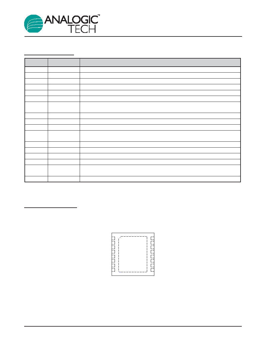
Pin Descriptions
Pin Configuration
TDFN44-16
(Top View)
C3-
C3+
OUT_FLASH
1
IN
C1+
C1-
CP
C2+
D4
D2
EN_FLSH
D1
D3
EN/SET
GND
C2-
8
5
6
7
2
3
4
10
16
15
14
13
12
11
9
Pin #
Symbol
Function
1
C3-
Flying capacitor 3 negative terminal. Connect a 1µF capacitor between C3- and C3+.
2
C3+
Flying capacitor 3 positive terminal.
3
OUT_FLASH
Flash output voltage. Requires 1µF capacitor connected between this pin and ground.
4
IN
Input power supply. Requires 1µF capacitor connected between this pin and ground.
5
C1+
Flying capacitor 1 positive terminal. Connect a 1µF capacitor between C1+ and C1-.
6
C1-
Flying capacitor 1 negative terminal.
7
CP
White LED charge pump output. Requires 1µF capacitor connected between this pin
and ground.
8
C2+
Flying capacitor 2 positive terminal. Connect a 1µF capacitor between C2+ and C3-.
9
C2-
Flying capacitor 2 negative terminal.
10
GND
Ground.
11
EN/SET
S
2
Cwire serial interface control pin for the white LED charge pump. This pin should not
be left floating.
12
D3
Current source output #3.
13
D1
Current source output #1.
14
D4
Current source output #4.
15
D2
Current source output #2.
16
EN_FLSH
Active high enable pin for the flash charge pump. When connected low, the charge
pump shuts down and consumes less than 1µA of current.
EP
Exposed paddle (bottom); connect to GND directly beneath package.
AAT2801
Multi-Mode Charge Pump for
White LED Backlight and Flash Applications
2
2801.2006.04.1.3

Absolute Maximum Ratings
1
Thermal Information
Symbol
Description
Value
Units
P
D
Maximum Power Dissipation
3, 4
2.0
mW
JA
Thermal Resistance
3
50
∞C/W
Symbol
Description
Value
Units
V
IN
Input Voltage
-0.3 to 6.0
V
V
EN/SET
EN/SET to GND Voltage
-0.3 to V
IN
+0.3
V
I
OUT
2
Maximum DC Output Current
120
mA
T
J
Operating Junction Temperature Range
-40 to 150
∞C
AAT2801
Multi-Mode Charge Pump for
White LED Backlight and Flash Applications
2801.2006.04.1.3
3
1. Stresses above those listed in Absolute Maximum Ratings may cause permanent damage to the device. Functional operation at condi-
tions other than the operating conditions specified is not implied. Only one Absolute Maximum Rating should be applied at any one time.
2. Based on long-term current density limitation.
3. Mounted on an FR4 board.
4. Derate 6.25mW/∞C above 25∞C.

Electrical Characteristics
1
C
IN
= C
CP
= C
F
= C1 = C2 = C3 = 1.0µF; T
A
= -40∞C to 85∞C, unless otherwise noted.
Symbol
Description
Conditions
Min Typ Max Units
Input Power Supply
V
IN
Operation Range
2.7
5.5
V
3.0
V
IN
5.5, No Load Current; V
OUT_FLSH
-
3.0
4.5
= 5V, EN/SET = GND, EN_FLSH = V
IN
I
CC
Operating Current
3.0
V
IN
5.5, EN/SET = V
IN
, EN_FLSH =
0.55
mA
GND, VD1:VD4 = 2.0V, CP = 1X
3.0
V
IN
5.5, No Load Current; EN/SET =
-
3.0
5.0
V
IN
, EN_FLSH = GND, CP = 1.5X
I
SHDN
Shutdown Current
EN_FLSH = EN/SET = 0
-
1.0
µA
I
DX
Output Current Accuracy
2
V
IN
= 3.5, Code = 32, T
A
= 25∞C
-10
10
%
I
(D-Match)
Current Matching
3
VD1:D4 = 3.6, V
IN
= 3.5V; LED Charge
-3.0 ±0.5
3.0
%
Pump Only
V
OUT
Flash Charge Pump Output
3.0V < V
IN
< 5V, I
OUT
= 120mA;
4.3
4.5
4.7
V
Voltage
EN_FLSH = V
IN
I
OUT
Maximum Continuous I
OUT
V
IN
= 3.6V; V
OUT
= 4.5V; EN_FLSH = V
IN
120
-
mA
Maximum Pulsed I
OUT
V
IN
= 3.6V; V
OUT
= 4.5V; I
Pulsed
< 500mS
250
-
CP
White LED Charge Pump
V
IN
= 3.5V, I
OUT(TOTAL)
= 120mA,
93
%
Section Efficiency
Measured from IN to CP
Charge Pump Section
T
SS
Soft-Start Time
Backlight Charge Pump
50
µs
Flash Charge Pump
200
F
CLK
Clock Frequency
1.0
MHz
EN/SET
V
EN(L)
Enable Threshold Low
-
0.4
V
V
EN(H)
Enable Threshold High
1.4
-
V
T
EN/SET LO
EN/SET Low Time
V
EN/SET
< 0.6V
0.3
75
µs
T
EN/SET HI MIN
Minimum EN/SET High Time V
EN/SET
> 1.4V
50
µs
T
EN/SET HI MAX
Maximum EN/SET High Time V
EN/SET
> 1.4V
-
75
µs
T
OFF
EN/SET Off Timeout
V
EN/SET
< 0.6V
-
500
µs
T
LAT
EN/SET Latch Timeout
V
EN/SET
> 1.4V
-
500
µs
I
EN/SET/EN_FLSH
Input Leakage
V
EN/SET/EN_FLSH
= 5V, V
IN
= 5V
-1.0
1.0
µA
AAT2801
Multi-Mode Charge Pump for
White LED Backlight and Flash Applications
4
2801.2006.04.1.3
1. The AAT2801 is guaranteed to meet performance specifications over the -40∞C to 85∞C operating temperature range and is assured
by design, characterization, and correlation with statistical process controls.
2. Codes 2 through 7 are guaranteed to be within ±15% of stated current level.
3. Current matching is defined as I
(D-Match)
= (I
D
- I
AVE
)/I
AVE
.

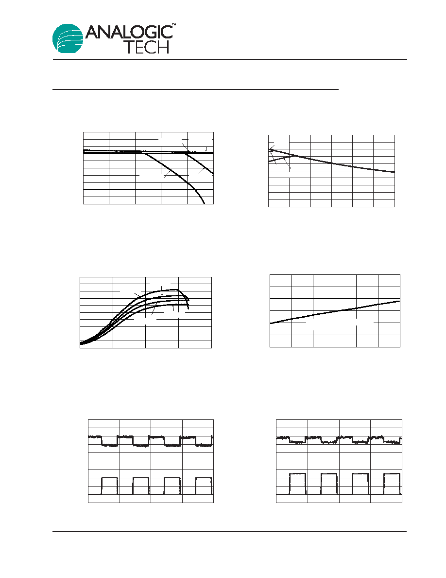
Typical Characteristics≠White LED Backlight Driver Section
V
IN
= 3.5V, C
IN
= 2.2µF, C
CP
= C1 = C2 = 1.0µF; T
A
= 25∞C, unless otherwise noted.
Operating Current
(Code 23; EN_FLSH On; I
OUT
= 100mA)
Input Voltage (V)
I
IN
(A)
0.0
1.0
2.0
3.0
4.0
5.0
6.0
7.0
8.0
2.7 2.9 3.1 3.3 3.5 3.7 3.9 4.1 4.3 4.5 4.7 4.9 5.1 5.3 5.5
V_D
X
= 3.3V
V_D
X
= 3.0V
Operating Current
(Code 23; EN_FLSH Off)
Input Voltage (V)
I
IN
(A)
0.0
1.0
2.0
3.0
4.0
5.0
2.7 2.9 3.1 3.3 3.5 3.7 3.9 4.1 4.3 4.5 4.7 4.9 5.1 5.3 5.5
V_D
X
= 3.3V
V_D
X
= 3.0V
Input Voltage (V)
Efficiency (%)
30
40
50
60
70
80
90
100
2.9 3.0 3.1 3.2 3.3 3.4 3.5 3.6 3.7 3.8 3.9 4.0 4.1 4.2
Code 32
Code 28
Code 26
Efficiency vs. V
IN
(D1-D2 = 3.5V; D3-D4 = 3.2V)
Efficiency vs. V
IN
(D1 = 3.5V; D2 = 3.3V; D3 = 3.2V; D4 = 3.0V)
Input Voltage (V)
Efficiency (%)
30
40
50
60
70
80
90
100
2.9 3.0 3.1 3.2 3.3 3.4 3.5 3.6 3.7 3.8 3.9 4.0 4.1 4.2
Code 32
Code 28
Code 26
Input Voltage (V)
Efficiency (%)
30
40
50
60
70
80
90
100
2.9 3.0 3.1 3.2 3.3 3.4 3.5 3.6 3.7 3.8 3.9 4.0 4.1 4.2
Efficiency vs. V
IN
(Code 26)
3.5V
F
3.0V
F
AAT2801
Multi-Mode Charge Pump for
White LED Backlight and Flash Applications
2801.2006.04.1.3
5

Typical Characteristics≠White LED Backlight Driver Section
V
IN
= 3.5V, C
IN
= 2.2µF, C
CP
= C1 = C2 = 1.0µF; T
A
= 25∞C, unless otherwise noted.
Flash Section Turn-On
(V
IN
= 3.5V; I
OUT
= 200mA; EN/SET = GND)
EN_FLSH
(2V/div)
V
OUT
(2V/div)
I
IN
(100mA/div)
Time (100µs/div)
Flash Section Turn-On
(V
IN
= 3.5V; I
OUT
= 100mA; EN/SET = GND)
EN_FLSH
(2V/div)
V
OUT
(2V/div)
I
IN
(100mA/div)
Time (100µs/div)
Turn-Off from Full-Scale 2X Mode
EN/SET
(2V/div)
V
DIODE
(2V/div)
I
IN
(200mA/div)
Time (100µs/div)
Turn-On to 1.5X Mode
(4x19mA Load)
Time (100µs/div)
EN/SET
(2V/div)
V
CP
(4V/div)
V
DIODE
(2V/div)
I
IN
(100mA/div)
Turn-On to 1X Mode
(4x30mA Load)
EN/SET
(2V/div)
V
CP
(4V/div)
V
DIODE
(2V/div)
I
IN
(100mA/div)
Time (100µs/div)
Turn-On to 1X Mode
(4x19mA Load)
EN/SET
(2V/div)
V
CP
(4V/div)
V
DIODE
(2V/div)
I
IN
(100mA/div)
Time (100µs/div)
AAT2801
Multi-Mode Charge Pump for
White LED Backlight and Flash Applications
6
2801.2006.04.1.3

Typical Characteristics≠White LED Backlight Driver Section
V
IN
= 3.5V, C
IN
= 2.2µF, C
CP
= C1 = C2 = 1.0µF; T
A
= 25∞C, unless otherwise noted.
Load Switch to Charge Pump
(1.5X Mode; 4x30mA Load)
V
IN
(1V/div)
V
CP
(4V/div)
V
DIODE
(500mV/div)
I
IN
(50mA/div)
Time (2ms/div)
Load Switch to Charge Pump
(1.5X Mode; 4x19mA Load)
V
IN
(1V/div)
V
CP
(4V/div)
V
DIODE
(500mV/div)
I
IN
(50mA/div)
Time (2ms/div)
Charge Pump to Load Switch
(2X Mode; 4x30mA Load)
V
IN
(500mV/div)
V
CP
(1V/div)
V
DIODE
(500mV/div)
I
IN
(50mA/div)
Time (5ms/div)
Charge Pump to Load Switch
(2X Mode; 4x19mA Load)
V
IN
(500mV/div)
V
CP
(1V/div)
V
DIODE
(500mV/div)
I
IN
(50mA/div)
Time (5ms/div)
Charge Pump to Load Switch
(1.5X Mode; 4x30mA Load)
V
IN
(500mV/div)
V
CP
(1V/div)
V
DIODE
(500mV/div)
I
IN
(50mA/div)
Time (5ms/div)
Charge Pump to Load Switch
(1.5X Mode; 4x19mA Load)
V
IN
(500mV/div)
V
CP
(1V/div)
V
DIODE
(500mV/div)
I
IN
(50mA/div)
Time (5ms/div)
AAT2801
Multi-Mode Charge Pump for
White LED Backlight and Flash Applications
2801.2006.04.1.3
7

AAT2801
Multi-Mode Charge Pump for
White LED Backlight and Flash Applications
8
2801.2006.04.1.3
Typical Characteristics≠White LED Backlight Driver Section
V
IN
= 3.5V, C
IN
= 2.2µF, C
CP
= C1 = C2 = 1.0µF; T
A
= 25∞C, unless otherwise noted.
Line Response
(I
OUT
= 100mA; I_D
X
= 4x19mA; 1.5X Mode)
V
CP
(0.5V/div)
V
IN
(0.5V/div)
V
F
(10mV/div)
V
DX
(20mV/div)
I
DX
(10mA/div)
Time (1ms/div)
Line Response
(1.5X Mode; 4x30mA Load)
V
IN
(0.5V/div)
V
LED
(20mV/div)
V
CP
(0.5V/div)
I
D
(10mA/div)
Time (1ms/div)
Line Response
(1.5X Mode; 4x19mA Load)
V
CP
(0.5V/div)
V
IN
(0.5V/div)
V
DX
(20mV/div)
I
DX
(10mA/div)
Time (1ms/div)
Line Response
(1X Mode; 4x30mA Load)
V
IN
(0.5V/div)
V
LED
(20mV/div)
V
CP
(0.5V/div)
I
D
(10mA/div)
Time (1ms/div)
Line Response
(1X Mode; 4x19mA Load)
V
IN
(0.5V/div)
V
LED
(20mV/div)
V
CP
(0.5V/div)
I
D
(10mA/div)
Time (1ms/div)

AAT2801
Multi-Mode Charge Pump for
White LED Backlight and Flash Applications
2801.2006.04.1.3
9
Typical Characteristics≠White LED Backlight Driver Section
V
IN
= 3.5V, C
IN
= 2.2µF, C
CP
= C1 = C2 = 1.0µF; T
A
= 25∞C, unless otherwise noted.
Input Voltage (V)
I
IN
(mA)
Input Current vs. Input Voltage
(4x30mA)
0
50
100
150
200
250
300
2.7
3.1
3.5
3.9
4.3
4.7
5.1
5.5
V
DIODE
= 3.0V
V
DIODE
= 3.4V
Input Voltage (V)
I
IN
(mA)
Input Current vs. Input Voltage
(4x10mA)
0
10
20
30
40
50
60
70
80
90
2.7
3.1
3.5
3.9
4.3
4.7
5.1
5.5
V
DIODE
= 3.4V
V
DIODE
= 3.0V
Operating Characteristics
(I_D
X
= 4x30mA; 1.5X Mode; I
OUT
= 100mA)
Time (1µs/div)
V
CP
(40mV/div)
V
F
(40mV/div)
V
DX
(20mV/div)
I
IN
(10mA/div)
Operating Characteristics
(I_D
X
= 4x30mA; 1.5X Mode)
Time (1µs/div)
V
CP
(40mV/div)
V
DX
(20mV/div)
I
IN
(10mA/div)
V
IN
= 3.5V
Operating Characteristics
(I_D
X
= 4x15mA; 1.5X Mode; I
OUT
= 100mA)
Time (1µs/div)
V
CP
(20mV/div)
V
F
(40mV/div)
V
DX
(20mV/div)
I
IN
(10mA/div)
V
IN
= 3.0V
Operating Characteristics
(I_D
X
= 4x15mA; 1.5X Mode)
Time (1µs/div)
V
CP
(20mV/div)
V
DX
(20mV/div)
I
IN
(10mA/div)
V
IN
= 3.0V

Typical Characteristics≠White LED Backlight Driver Section
V
IN
= 3.5V, C
IN
= 2.2µF, C
CP
= C1 = C2 = 1.0µF; T
A
= 25∞C, unless otherwise noted.
V
IH
and V
IL
vs. V
IN
Input Voltage (V)
0.600
0.625
0.650
0.675
0.700
0.725
0.750
0.775
0.800
0.825
0.850
2.5
3.0
3.5
4.0
4.5
5.0
5.5
V
IH
V
IL
Input Voltage (V)
I
DIODE
(mA)
Diode Current vs. Input Voltage
(30mA; 15mA settings)
10
15
20
25
30
35
40
2.7
3.1
3.5
3.9
4.3
4.7
5.1
5.5
V
DIODE
= 3.4V
V
DIODE
= 3.4V
AAT2801
Multi-Mode Charge Pump for
White LED Backlight and Flash Applications
10
2801.2006.04.1.3

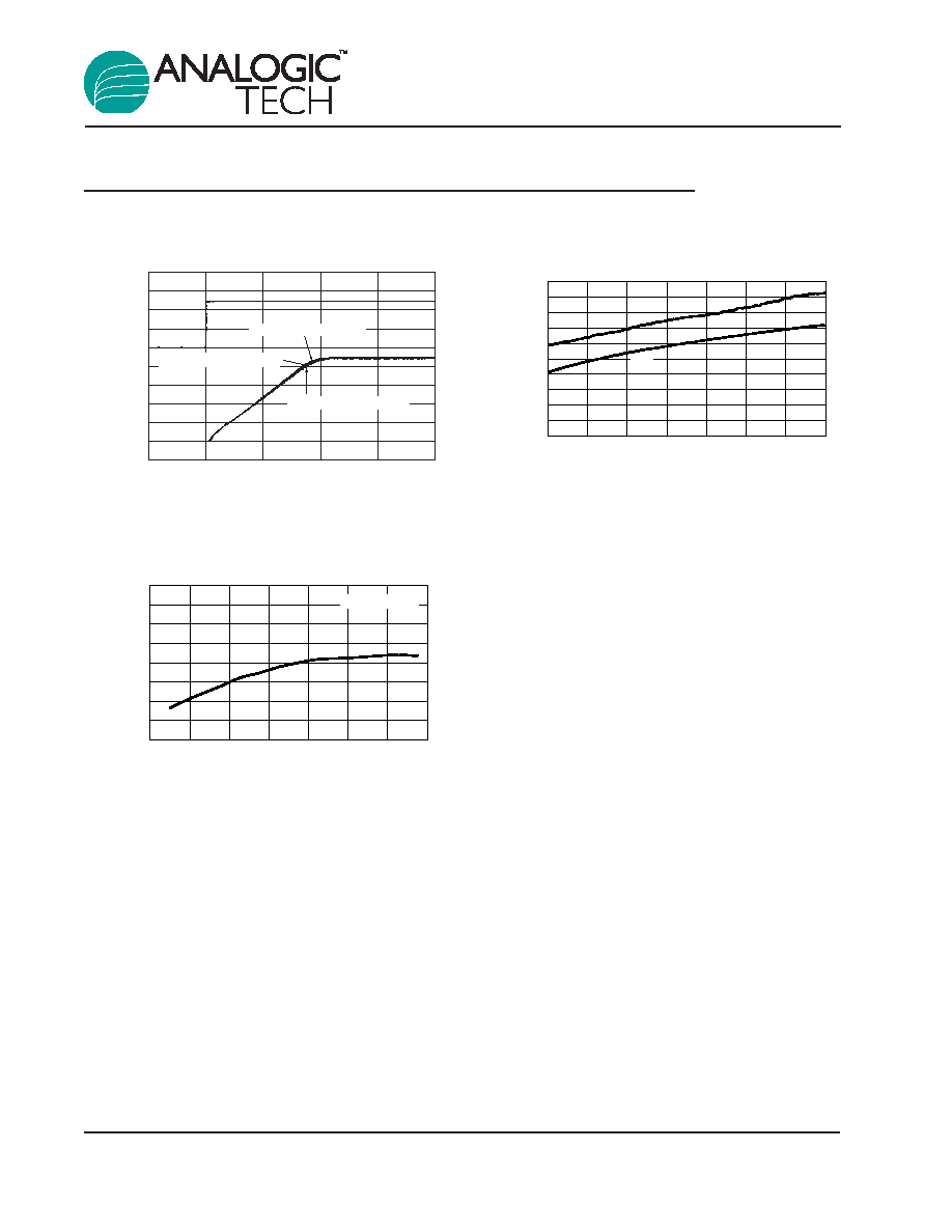
Typical Characteristics≠Flash Driver Charge Pump Section
V
IN
= 3.5V, C
IN
= 2.2µF, C
3
= C
F
= 1.0µF, T
A
= 25∞C, unless otherwise noted.
Load Response
(50mA Load)
V
OUT
(10mV/div)
I
OUT
(20mA/div)
V
IN
= 3.5V
Time (5ms/div)
Load Response
(100mA Load)
V
OUT
(10mV/div)
I
OUT
(50mA/div)
V
IN
= 3.5V
Time (5ms/div)
Maximum Current Pulse vs. Supply Voltage
Supply Voltage (V)
Maximum Current Pulse (mA)
0
100
200
300
400
500
600
3.0
3.2
3.4
3.6
3.8
4.0
4.2
One-shot pulse duration = 250ms
V
OUT
> 4.0V
Efficiency vs. Load Current
Load Current (mA)
Efficiency (%)
0
10
20
30
40
50
60
70
80
90
100
0.1
1.0
10
100
1000
V
IN
= 2.7V
V
IN
= 3.0V
V
IN
= 3.3V
V
IN
= 3.6V
Efficiency vs. Supply Voltage
Supply Voltage (V)
Efficiency (%)
0
10
20
30
40
50
60
70
80
90
100
2.7
3.0
3.3
3.6
3.9
4.2
4.5
50mA
100mA
150mA
Output Voltage vs. Output Current
Output Current (mA)
Output Voltage (V)
3.0
3.2
3.4
3.6
3.8
4.0
4.2
4.4
4.6
4.8
5.0
0
40
80
120
160
200
V
IN
=3.3
V
IN
=3.6
V
IN
= 2.7
V
IN
= 3.0
AAT2801
Multi-Mode Charge Pump for
White LED Backlight and Flash Applications
2801.2006.04.1.3
11

Typical Characteristics≠Flash Driver Charge Pump Section
V
IN
= 3.5V, C
IN
= 2.2µF, C
3
= C
F
= 1.0µF, T
A
= 25∞C, unless otherwise noted.
Normalized Output Voltage vs. Temperature
Temperature (
∞C)
Normalized Output Voltage (%)
-2.0
-1.5
-1.0
-0.5
0.0
0.5
1.0
1.5
2.0
-50
-30
-10
10
30
50
70
90
I
OUT
= 25mA
V
EN
Threshold vs. Supply Voltage
Supply Voltage (V)
V
EN
Threshold (V)
0.50
0.55
0.60
0.65
0.70
0.75
0.80
0.85
0.90
0.95
1.00
2.7
3.1
3.5
3.9
4.3
4.7
5.1
5.5
V
IL
V
IH
Startup
Time (100µs/div)
V
OUT
(1V/div)
ENABLE
(1V/div)
I
LOAD
= 100mA @ V
IN
= 3.0V
I
LOAD
= 150mA @ V
IN
= 3.3V
I
LOAD
= 150mA @ V
IN
= 3.3V
AAT2801
Multi-Mode Charge Pump for
White LED Backlight and Flash Applications
12
2801.2006.04.1.3

AAT2801
Multi-Mode Charge Pump for
White LED Backlight and Flash Applications
2801.2006.04.1.3
13
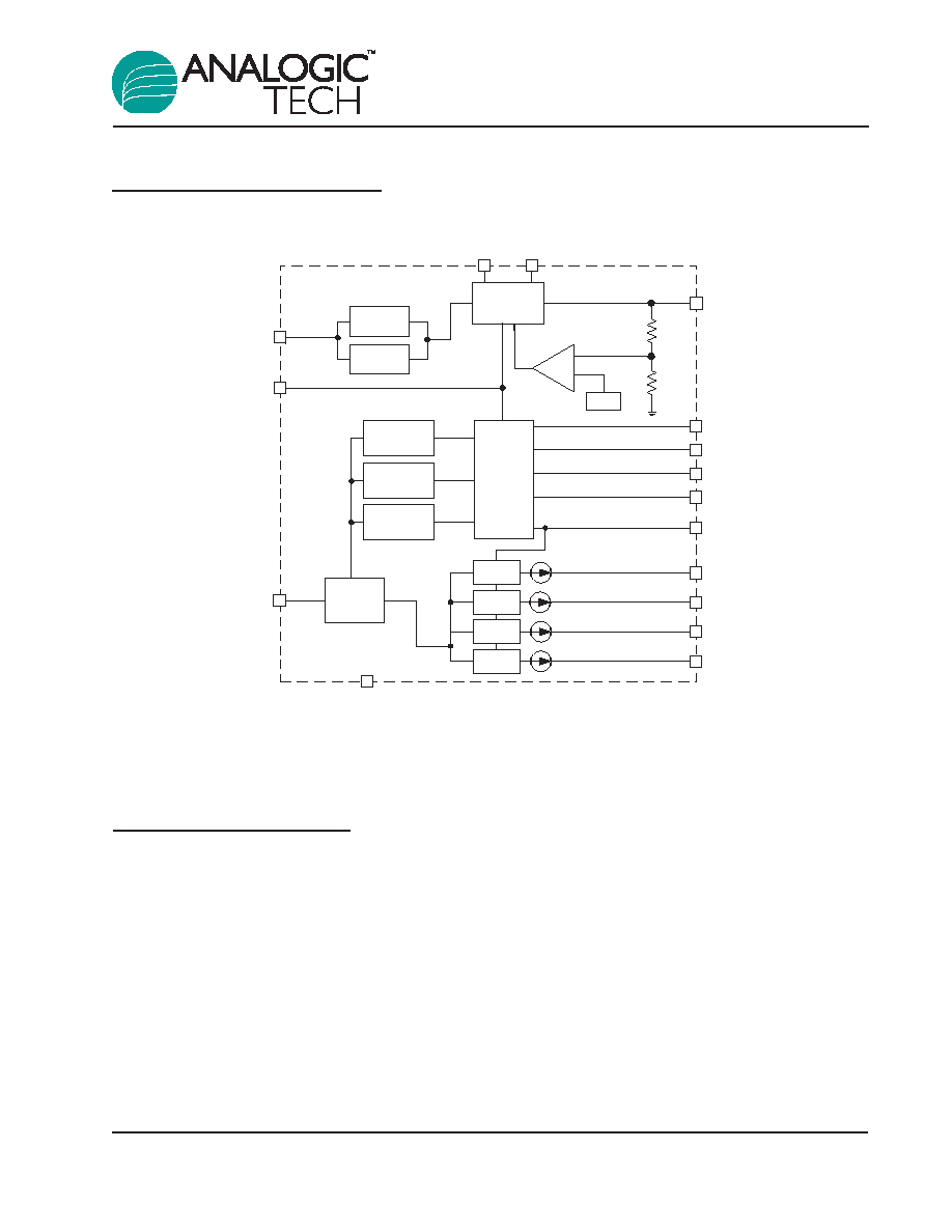
Functional Block Diagram
1X
1.5X
2X
Charge
Pump
Soft-Start
Control
1MHz
Oscillator
Voltage
Reference
C1+
C1-
C2+
C2-
CP
D1
D2
D3
D4
GND
EN/SET
IN
Control
Logic
D/A
D/A
D/A
D/A
OUT_FLSH
V
REF
Soft Start
1MHz
Oscillator
2X CP
C3
+
C3
-
EN_FLSH
Functional Description
The AAT2801 is a dual charge pump for white
LED and flash applications. The charge pump for
white LED application is a tri-mode load switch
(1X) and high efficiency (1.5X or 2X) charge
pump device intended for white LED backlight
applications. To maximize power conversion effi-
ciency, an internal sensing circuit monitors the
voltage required on each constant current source
output and sets the load switch and charge pump
modes based on the input battery voltage and the
current source output voltage. As the battery dis-
charges over time, the AAT2801 charge pump is
enabled when any of the four current source out-
puts nears dropout. The charge pump initially
starts in 1.5X mode. If the charge pump output
drops enough for any current source output to
become close to dropout, the charge pump will
automatically transition to 2X mode.
The second section of the AAT2801 contains a
voltage doubling charge pump to supply flash LED
functions. The voltage doubling charge pump pro-
vides a 4.5V regulated output and has an inde-
pendent enable control.
AutoBias Technology
Each of the four current source outputs for the
white LED backlight charge pump section is inde-
pendently switched between the battery input (1X)
or the charge pump output (1.5X or 2X), depending

AAT2801
Multi-Mode Charge Pump for
White LED Backlight and Flash Applications
14
2801.2006.04.1.3
14
2801.2006.04.1.3
on the voltage at the current source output. Since
the LED to LED V
F
can vary as much as 1 volt, this
function significantly enhances overall efficiency of
the white LED backlight charge pump section when
the battery input voltage level is greater than the
voltage required at any current source output.
Flash Driver
For flash applications, the voltage doubling
charge pump section is used to support the high
current demand required by the application.
Charge pump regulation is achieved by sensing
the output voltage through an internal resistor
divider network. The free running charge pump
switching frequency is approximately 1MHz. The
charge pump is designed to deliver up to 120mA
of continuous current and 250mA of pulsed cur-
rent for up to 500ms.
The AAT2801 requires only six external compo-
nents: three 1µF ceramic capacitors for the
charge pump flying capacitors (C1, C2 and C3),
one 1µF ceramic input capacitor (C
IN
), one 1µF
ceramic charge pump output capacitor (C
CP
), and
one 1µF for the flash output (C
F
). The four con-
stant current outputs (D1 to D4) drive four individ-
ual LEDs with a maximum current of 30mA each.
The EN/SET S
2
Cwire serial interface enables the
AAT2801 and sets the current source magni-
tudes. A separate flash enable pin (EN_FLSH) is
provided to independently control the flash charge
pump circuit.
Applications Information--
White LED Backlight Section
Constant Current Output Level Settings
The constant current source amplitudes for D1 to D4
are set via the serial interface according to a loga-
rithmic scale, where each code is 1dB greater than
the previous code. In this manner, LED brightness
appears linear with each increasing code count.
Because the outputs D1 to D4 are true independent
constant current sources, the voltage observed on
any single given output will be determined by the
actual forward voltage (V
F
) for the LED being driven.
Since the output current of the AAT2801 is program-
mable, no PWM (pulse width modulation) or addi-
tional control circuitry is needed to control LED
brightness. This feature greatly reduces the burden
on a microcontroller or system IC to manage LED or
display brightness, allowing the user to "set it and
forget it." With its high-speed serial interface (1MHz
data rate), the output current of the AAT2801 can be
changed successively to brighten or dim LEDs in
smooth transitions (e.g., to fade-out) or in abrupt
steps, giving the user complete programmability and
real-time control of LED brightness.
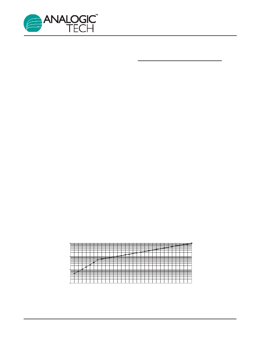
The 32 individual current level settings are each
approximately 1dB apart (see Current Level
Settings below). Code 32 is full scale; Code 2 is full
scale attenuated by 31dB; and Code 1 is reserved
as a "no current" setting.
Normalized Current Level Settings
Code
Current (mA)
0.00
0.01
0.10
1.00
1
2
3
4
5
6 7
8
9 10 11 12 13 14 15 16 17 18 19 20 21 22 23 24 25 26 27 28 29 30 31 32

AAT2801
Multi-Mode Charge Pump for
White LED Backlight and Flash Applications
2801.2006.04.1.3
15
S
2
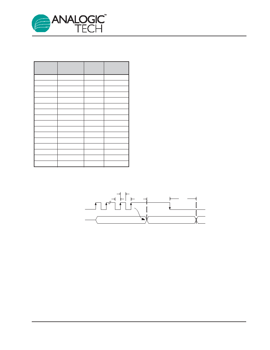
Cwire Serial Interface Timing Diagram
1
EN/SET
2
n-1
n <= 32
Data Reg
0
n
0
T
HI
T
LO
T
LAT
T
OFF
Constant Current Source Output
Nominal Programming Levels (mA)
S
2
Cwire Serial Interface
The current source output magnitude is controlled
by the EN/SET pin, using AnalogicTech's S
2
Cwire
interface. The interface records rising edges of
the EN/SET pin and decodes them into 32 indi-
vidual current level settings each 1dB apart with
Code 1 reserved for no current. Once EN/SET
has been held in the logic high state for time T
LAT
,
the programmed current is seen at the current
source outputs, and the internal data register is
reset to 0. For subsequent current level pro-
gramming, the number of rising edges correspon-
ding to the desired code must be entered on the
EN/SET pin.
When EN/SET is held low for an amount of time
greater than T
OFF
, the AAT2801 enters into shut-
down mode and draws less than 1µA from V
IN
.
The internal data register is reset to 0 during shut-
down.
I
OUT
(typ)
I
OUT
(typ)
Code
(mA)
Code
(mA)
1
0.0
17
5.1
2
0.1
18
5.6
3
0.2
19
6.4
4
0.4
20
7.2
5
0.5
21
8.1
6
0.7
22
9.2
7
1.1
23
10.2
8
1.8
24
11.5
9
2.0
25
13.1
10
2.2
26
14.7
11
2.5
27
16.6
12
2.8
28
18.6
13
3.2
29
20.9
14
3.5
30
23.6
15
4.0
31
26.6
16
4.5
32
30.0
Termination of Unused Current Source
Outputs
If any outputs (D1 to D4) are not used, they should
be terminated by connecting the respective unused
output directly to ground. This is required to assure
correct charge pump mode operation. If a given
unused output is not terminated to ground, it will
appear to the respective output's feedback control
as an infinite impedance load and the unused con-
stant current source will be set to maximum volt-
age. Although no current flows from the unused
current source, the voltage sensed at that node
could force the charge pump control to activate the
charge pump when it is not necessary. To prevent
this effect, simply connect unused constant current
source outputs to ground.
LED Selection
The AAT2801 is specifically intended for driving
white LEDs. However, the device design will allow
the AAT2801 to drive most types of LEDs with for-
ward voltage specifications ranging from 2.0V to
4.3V. Since the D1 to D4 output current sources
are matched with negligible voltage dependence,
the LED brightness will be matched regardless of
the specific LED forward voltage (V
F
) levels.

AAT2801
Multi-Mode Charge Pump for
White LED Backlight and Flash Applications
16
2801.2006.04.1.3
Applications Information--
White LED Charge Pump Section
Power Efficiency and Device
Evaluation
The charge pump efficiency discussion in the fol-
lowing sections only accounts for efficiency of the
charge pump section itself. Due to the unique circuit
architecture and design of the AAT2801, it is very
difficult to measure efficiency in terms of a percent
value comparing input power over output power.
Since the AAT2801 outputs are pure constant cur-
rent sources and typically drive individual loads, it
is difficult to measure the output voltage for a given
output (D1 to D4) to derive an overall output power
measurement. For any given application, white
LED forward voltage levels can differ, yet the out-
put drive current will be maintained as a constant.
This makes quantifying output power a difficult task
when taken in the context of comparing to other white
LED driver circuit topologies. A better way to quantify
total device efficiency is to observe the total input
power to the device for a given LED current drive
level. The best white LED driver for a given applica-
tion should be based on trade-offs of size, external
components count, reliability, operating range, and
total energy usage...not just "% efficiency."
Efficiency of the AAT2801 can be quantified under
very specific conditions and is dependent upon the
input voltage versus the output voltage seen across
the loads applied to outputs D1 through D4 for a
given constant current setting. Depending upon the
case of V
IN
being greater than the specific voltage
seen across the load on D1 to D4, the device will
operate in load switch mode. If the voltage seen on
any constant current source output is less than V
IN
,
then the device will operate in 1.5X or 2X charge
pump mode. Each of these modes will yield differ-
ent efficiency values. One should refer to the fol-
lowing two sections for explanations for each opera-
tional mode.
Load Switch Mode Efficiency
The AAT2801 load switch mode is operational at all
times and functions alone to enhance device power
conversion efficiency when the condition exists
where V
IN
is greater than voltage across the load
connected to the constant current source outputs.
When in load switch mode, the voltage conversion
efficiency is defined as output power divided by
input power:
The expression to define the ideal efficiency (
)
can be rewritten as:
-or-
Charge Pump Section Efficiency
The AAT2801 contains a dual mode fractional and
voltage doubling charge pump which will boost the
input supply voltage in the event where V
IN
is less
than the voltage required on the constant current
source outputs. The efficiency (
) can be simply
defined as a linear voltage regulator with an effec-
tive output voltage that is equal to one and one half
or two times the input voltage. Efficiency (
) for an
ideal 1.5X charge pump can typically be expressed
as the output power divided by the input power.
=
P
OUT
P
IN
(%) = 100
V
OUT
V
IN
= P
OUT
= V
OUT
◊ I
OUT
= V
OUT
P
IN
V
IN
◊ I
OUT
V
IN
=
P
OUT
P
IN

AAT2801
Multi-Mode Charge Pump for
White LED Backlight and Flash Applications
2801.2006.04.1.3
17
In addition, with an ideal 1.5X charge pump, the
output current may be expressed as 2/3 of the
input current. The expression to define the ideal
efficiency (
) can be rewritten as:
-or-
For the voltage doubling charge pump mode, the
expression to define the ideal efficiency (
) can be
rewritten as:
-or-
The flash driver charge pump section utilizes a 2X
voltage doubling topology; thus, the same efficien-
cy equation may be used to calculate the flash
charge pump efficiency.
Capacitor Selection
Careful selection of the six external capacitors C
IN
,
C1, C2, C3, C
CP
, and C
F
is important because they
will affect turn-on time, output ripple, and transient
performance. Optimum performance will be
obtained when low equivalent series resistance
(ESR) ceramic capacitors are used. In general,
low ESR may be defined as less than 100m
. A
value of 1µF for all six capacitors is a good starting
point when choosing capacitors. If the LED current
sources are only programmed for light current lev-
els, then the capacitor size may be decreased.
Conversely, if the flash driver charge pump is to
provide the maximum flash current of 250mA, C
IN
may be increased to 2.2µF or more to reduce the
load transient effects of the flash driver output.
Capacitor Characteristics
Ceramic composition capacitors are highly recom-
mended over all other types of capacitors for use
with the AAT2801. Ceramic capacitors offer many
advantages over their tantalum and aluminum elec-
trolytic counterparts. A ceramic capacitor typically
has very low ESR, is lowest cost, has a smaller
PCB footprint, and is non-polarized. Low ESR
ceramic capacitors help maximize charge pump
transient response. Since ceramic capacitors are
non-polarized, they are not prone to incorrect con-
nection damage.
Thermal Protection
The AAT2801 has a thermal protection circuit that
will shut down the charge pump if the die tempera-
ture rises above the thermal limit.
Flash LED Driver
The AAT2801 flash driver charge pump circuit can
source 250mA for pulsed loads up to 500ms from
an input supply as low as 3.3V. This makes the
device well suited for low-cost flash LED driver
applications in portable products. Typically the
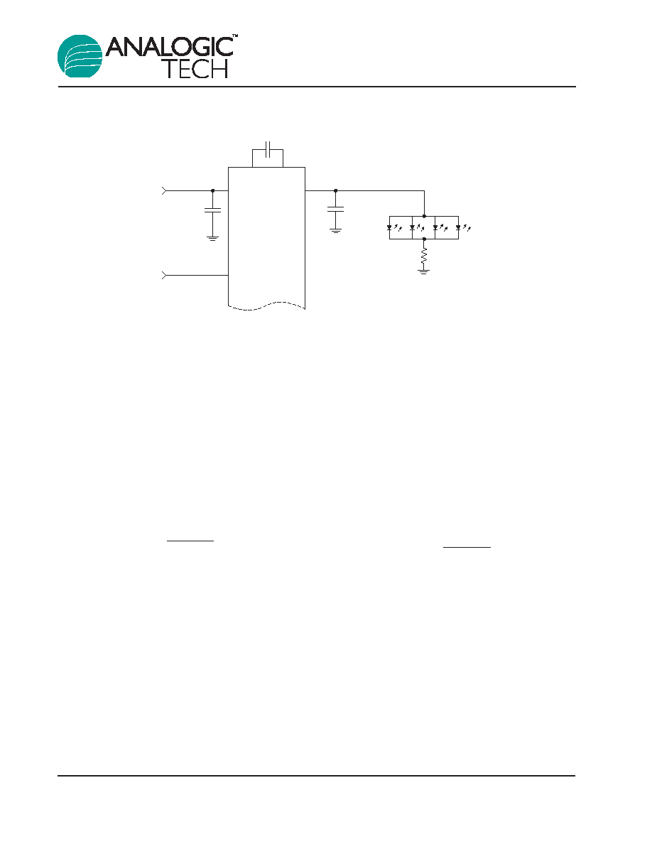
4.5V flash output (OUT_FLSH) version of the
AAT2801 should be selected for photo flash LED
applications, as it can maintain better voltage regu-
lation at higher pulsed load current levels (refer to
Figure 1). The limitation of this option is that the
greatest flash LED forward voltage (V
F
) that can be
driven is 4.5V at the maximum set forward current
(I
F
) for the application. Flash LEDs with forward
voltage (V
F
) levels up to 5.0V can be driven by the
AAT2801 5.0V output option. However, the maxi-
mum current for a 500ms pulse will be reduced.
Refer to the Typical Characteristics flash driver
curves for peak output current levels for a given
minimum input voltage.
(%) = 100
V
OUT
2V
IN
= P
OUT
= V
OUT
◊ I
OUT
= V
OUT
P
IN
V
IN
◊ 2I
OUT
2V
IN
(%) = 100
V
OUT
1.5V
IN
= P
OUT
= V
OUT
◊ I
OUT
= V
OUT
P
IN
V
IN
◊ 1.5I
OUT
1.5V
IN

AAT2801
Multi-Mode Charge Pump for
White LED Backlight and Flash Applications
18
2801.2006.04.1.3
The forward current (I
F
) through the flash LED may
be determined with the use of a series ballast resis-
tor. The typical forward voltage (V
F
) for the flash
LED in a given application should be derived from
the LED manufacturer's datasheet for the desired
forward current (I
F
) of the flash application. Once
the forward current has been determined, the flash
ballast resistor can be calculated using the follow-
ing equation:
Where:
R
B
= Flash ballast resistor value in ohms (
)
V
OUT
= Regulated charge pump output voltage
(typically 4.5V)
V
F
= Flash LED forward voltage at the
desired forward current
I
F
= Desired flash LED forward current
The flash LED function can be controlled by the
AAT2801 flash enable (EN_FLSH) pin in most
applications. The device start-up time into a maxi-
mum load is about 200µs, thus eliminating the
need for pre-flash control synchronization.
If a "light" or "movie" mode is also needed along
with the flash function, this can be accomplished
with the addition of a second ballast resistor with a
flash function gating MOSFET switch as shown in
Figure 2. Refer to the following equations for the
calculation of flash and light resistors, R
B
and R
L
.
Where:
R
L
= Light mode ballast resistor value in
ohms (
)
V
OUT
= Regulated charge pump output voltage
(typically 4.5V)
V
F
= Flash LED forward voltage at the
desired forward current
I
F
= Desired flash LED forward current in
the "light" mode
R
L
=
(V
OUT
- V
F
)
I
F
R
B
=
(V
OUT
- V
F
)
I
F
Figure 1: Flash LED Application.
AAT2801
IN
EN_FLSH
OUT_FLSH
4.5V
C
F
C
IN
R
B
1F
1F
1F
C
3
C3+
C3-
V
IN
Flash Enable
Flash LED

Where:
R
B
= Flash ballast resistor value in ohms (
)
R
DS
= Flash gating mosfet on resistance
V
OUT
= Regulated charge pump output voltage
(typically 4.5V)
V
F
= Flash LED forward voltage at the
desired forward current
I
F
= Desired flash LED forward current
R
B
=
- R
DS
(V
OUT
- V
F
)
I
F
AAT2801
Multi-Mode Charge Pump for
White LED Backlight and Flash Applications
2801.2006.04.1.3
19
Figure 2: Flash LED Driver with Gated Flash Application.
AAT2801
IN
C3+
C3-
EN_FLSH
OUT_FLSH
4.5V
C
OUT
C
IN
R
L
R
B
1F
1F
1F
C
3
V
IN
Flash Enable
Flash Enable
Flash LED

Ordering Information
Package Information
All dimensions in millimeters.
Index Area
(D/2 x E/2)
Detail "A"
Detail "B"
Top View
Bottom View
Detail "A"
Side View
Option A:
C0.30 (4x) max
Chamfered corner
Option B:
R0.30 (4x) max
Round corner
Detail "B"
0.16
Pin 1 Indicator
(optional)
0.1 REF
4.00 ± 0.05
2.60 ± 0.05
4.00
±
0.05
3.30
±
0.05
0.8
+
0.05 -0.20
0.05 ± 0.05
0.229
±
0.051
7.5∞ ± 7.5∞
0.375 ± 0.125
0.3 ± 0.10
0.45
±
0.05
0.23
±
0.05
0.075 ± 0.075
Output Voltage
Package
Marking
1
Part Number (Tape and Reel)
2
4.5V
TDFN44-16
MSXYY
AAT2801IXN-4.5-T1
5.0V
TDFN44-16
AAT2801IXN-5.0-T1
AAT2801
Multi-Mode Charge Pump for
White LED Backlight and Flash Applications
20
2801.2006.04.1.3
Advanced Analogic Technologies, Inc.
830 E. Arques Avenue, Sunnyvale, CA 94085
Phone (408) 737-4600
Fax (408) 737-4611
1. XYY = assembly and date code.
2. Sample stock is generally held on part numbers listed in BOLD.
© Advanced Analogic Technologies, Inc.
AnalogicTech cannot assume responsibility for use of any circuitry other than circuitry entirely embodied in an AnalogicTech product. No circuit patent licenses, copyrights, mask work rights,
or other intellectual property rights are implied. AnalogicTech reserves the right to make changes to their products or specifications or to discontinue any product or service without notice.
Customers are advised to obtain the latest version of relevant information to verify, before placing orders, that information being relied on is current and complete. All products are sold sub-
ject to the terms and conditions of sale supplied at the time of order acknowledgement, including those pertaining to warranty, patent infringement, and limitation of liability. AnalogicTech
warrants performance of its semiconductor products to the specifications applicable at the time of sale in accordance with AnalogicTech's standard warranty. Testing and other quality con-
trol techniques are utilized to the extent AnalogicTech deems necessary to support this warranty. Specific testing of all parameters of each device is not necessarily performed.
AnalogicTech and the AnalogicTech logo are trademarks of Advanced Analogic Technologies Incorporated. All other brand and product names appearing in this document are regis-
tered trademarks or trademarks of their respective holders.

