AAT2805
Dual High Efficiency Charge Pump
for White LED and Flash Applications
2805.2006.04.1.7
1
ChargePump
TM
General Description
The AAT2805 is a dual charge pump designed to
support both the white LED backlight and flash appli-
cations for systems operating with lithium-ion/poly-
mer batteries. The backlight charge pump is capable
of driving up to four LEDs at a total of 120mA. The
current sinks may be operated individually or in par-
allel for driving higher current LEDs. To maximize
power efficiency, the charge pump operates in 1X,
1.5X, or 2X mode, where the mode of operation is
automatically selected by comparing the forward
voltage of each LED with the input voltage.
AnalogicTech's AS
2
CwireTM (Advanced Simple Serial
ControlTM) serial digital input is used to enable, dis-
able, and set current for each LED with a 16-level
logarithmic scale plus four low-current settings down
to 50µA for optimized efficiency, with a typical oper-
ating quiescent current of less than 50µA.
The flash charge pump is a charge pump doubler
with a regulated output voltage. It is designed to
deliver 120mA of continuous current and up to
250mA of pulsed current. It has an independent
enable pin for improved power savings.
The AAT2805 has thermal protection and built-in
soft-start circuitry. A low-current shutdown feature
disconnects the load from V
IN
and reduces quiescent
current to less than 1µA.
The AAT2805 is available in a Pb-free, space-saving,
thermally-enhanced TDFN44-16 package and is
rated over the -40∞C to +85∞C temperature range.
Features
∑
V
IN
Range: 2.7V to 5.5V
∑
Dual Charge Pump to Support Backlight and
Flash LEDs
∑
Backlight Charge Pump:
-- Regulated Current
-- Four Current Sink Inputs
-- AS
2
Cwire Brightness Control
-- Tri-Mode Charge Pump
-- Maximum 30mA of Current Per Input
-- Low I
Q
(50µA) in Light Load Mode
∑
Flash Charge Pump:
-- Regulated Output Voltage
-- Up to 250mA of Pulsed Current
∑
Independent Backlight/Flash Control
∑
Low Noise 1MHz Constant Frequency
Operation
∑
Automatic Soft-Start
∑
No Inductors
∑
Available in TDFN44-16 Package
Applications
∑
Color (RGB) Lighting
∑
White LED Backlighting
∑
White LED Photo Flash
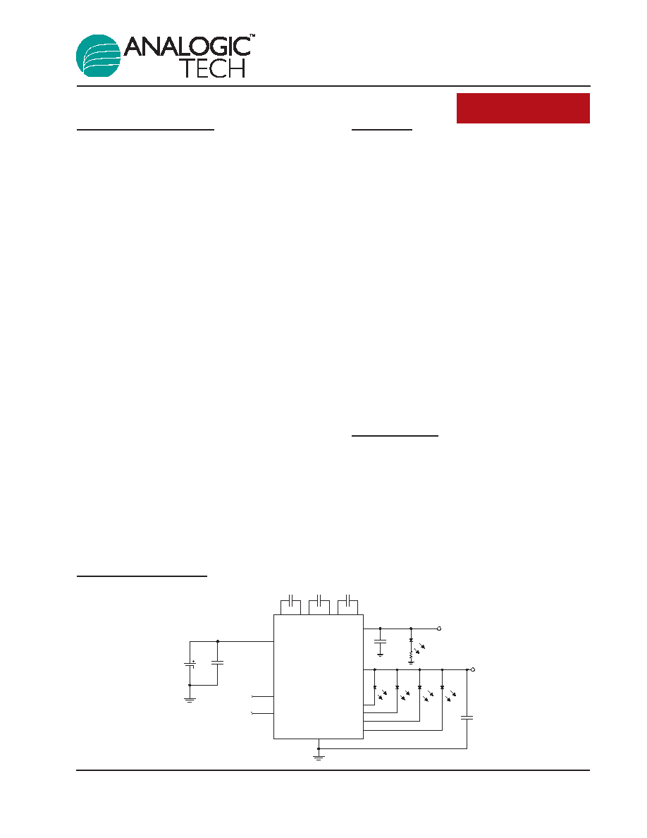
Typical Application
AAT2805
C
IN
1F
V
IN
C
OUT
1F
EN/SET
C1
1F
D3
D2
D1
VIN
C1+ C1- C2+ C2- C3+ C3-
D2
GND
Backlight
C2
1F
C3
1F
Flash
VOUT_FL
VOUT_BL
C
OUT
1F
EN_FLSH
EN/SET
EN_FLSH
D1
D3
D4
V
OUT_FLASH
D4

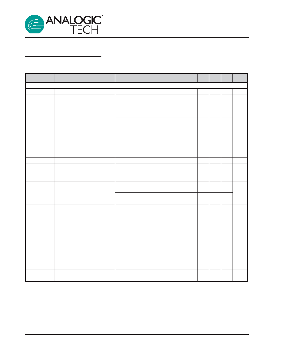
Pin Descriptions
Pin Configuration
TDFN44-16
(Top View)
VOUT_FL
VIN
D4
C3-
C3+
3
D3
D2
D1
C2+
VOUT_BL
C1-
EN_FLSH
C2-
C1+
EN/SET
GND
4
5
1
2
6
7
8
14
13
12
16
15
11
10
9
Pin #
Symbol
Function
1
C3-
Flying capacitor 3 negative terminal.
2
C3+
Flying capacitor 3 positive terminal. Connect a 1µF capacitor between C3+ and C3-.
3
VOUT_FL
Regulated output voltage for flash LED. Requires 1µF capacitor connected between this
pin and ground.
4
VIN
Input power supply. Requires 1µF capacitor connected between this pin and ground.
5
D4
Current sink input 4.
6
D3
Current sink input 3.
7
D2
Current sink input 2.
8
D1
Current sink input 1.
9
GND
Ground.
10
EN/SET
AS
2
Cwire serial interface control pin. It is used to enable/disable the backlight charge
pump and to control the brightness of the white LEDs.
11
C1+
Flying capacitor 1 positive terminal. Connect a 1µF capacitor between C1+ and C1-.
12
C1-
Flying capacitor 1 negative terminal.
13
VOUT_BL
Regulated output voltage for white LED. Requires 1µF capacitor connected between this
pin and ground.
14
C2+
Flying capacitor 2 positive terminal. Connect a 1µF capacitor between C2+ and C2-.
15
C2-
Flying capacitor 2 negative terminal.
16
EN_FLSH
Enable/disable pin for the flash charge pump.
EP
Exposed paddle (bottom); connect to GND directly beneath package.
AAT2805
Dual High Efficiency Charge Pump
for White LED and Flash Applications
2
2805.2006.04.1.7

Absolute Maximum Ratings
1
Thermal Information
2
Symbol
Description
Value
Units
P
D
Maximum Power Dissipation
3
2.0
W
JA
Maximum Thermal Resistance
50
∞C/W
Symbol
Description
Value
Units
V
IN
Input Voltage
-0.3 to 6.0
V
V
EN/SET
; EN_FL
EN/SET; EN_FL to GND Voltage
-0.3 to V
IN
+ 0.3
V
T
LEAD
Maximum Soldering Temperature (at leads, 10 sec)
300
∞C
AAT2805
Dual High Efficiency Charge Pump
for White LED and Flash Applications
2805.2006.04.1.7
3
1. Stresses above those listed in Absolute Maximum Ratings may cause permanent damage to the device. Functional operation at condi-
tions other than the operating conditions specified is not implied. Only one Absolute Maximum Rating should be applied at any one time.
2. Mounted on an FR4 board.
3. Derate 6.25mW/∞C above 25∞C.
Electrical Characteristics
1
V
IN
= 3.6V; C
IN
= C
OUT
= C
1
= C
2
= C
3
= 1.0µF; T
A
= -40∞C to +85∞C, unless otherwise noted.
Typical values are T
A
= 25∞C.
Symbol
Description
Conditions
Min Typ Max Units
Input Power Supply
V
IN
Operation Range
2.7
5.5
V
1X Mode, 3.0
V
IN
5.5, Active, No Load
0.3
1
Current; EN_FLSH = GND, EN/SET = V
IN
1.5X Mode, 3.0
V
IN
5.5, Active, No Load
1.0
3.0
Current; EN_FLSH = GND, EN/SET = V
IN
mA
I
CC
Operating Current
2X Mode, 3.0
V
IN
5.5, Active, No Load
1.0
3.0
Current; EN_FLSH = GND, EN/SET = V
IN
EN_FLSH = GND, 50µA Output Setting,
50
µA
1X Mode
3.0
V
IN
5.5, No Load Current;
2.0
4.5
mA
EN_FLSH = V
IN
, EN/SET = GND
I
SHDN
Shutdown Current
EN_FLSH = EN/SET = 0
1.0
µA
I
DX
Input Current Accuracy
2, 3
I
SET
= 30mA; T
A
= 25∞C
-10
10
%
I
(D-Match)
Current Matching Between
VD1:D4 = 3.6, V
IN
= 3.5V
0.5
%
Any Two Current Sink Inputs
2, 4
R
SINK
Sink Switch Impedance (each)
2
7
3.0V < V
IN
< 5V, I
OUT
= 100mA;
4.32 4.5 4.68
V
OUT_FL
Flash Charge Pump Output
EN_FLSH = V
IN
V
Voltage
5
3.0V < V
IN
< 5V, I
OUT
= 150mA;
4.3 4.5
4.7
EN_FLSH = V
IN
I
OUT_FL
Maximum Continuous I
OUT
5
V
IN
= 3.6V; V
OUT
= 4.5V; EN_FLSH = V
IN
120
mA
Maximum Pulsed I
OUT
5
V
IN
= 3.6V; V
OUT
= 4.5V; I
PULSED
< 500ms
250
T
SS
Soft-Start Time
100
µs
F
CLK
Clock Frequency
1.0
MHz
V
EN(L)
Enable Threshold Low
0.4
V
V
EN(H)
Enable Threshold High
1.4
V
T
EN/SET LO
EN/SET Low Time
V
EN/SET
< 0.6V
0.3
75
µs
T
EN/SET_HI_MIN
Minimum EN/SET High Time
V
EN/SET
> 1.4V
50
ns
T
EN/SET_HI_MAX
Maximum EN/SET High Time
75
µs
T
OFF
EN/SET Off Timeout
6
V
EN/SET
< 0.6V
500
µs
T
LAT
EN/SET Latch Timeout
7
V
EN/SET
> 1.4V
500
µs
I
I
Enable and EN/SET Input
V
EN/SET
= V
EN_FLSH
= V
IN
-1.0
1.0
µA
Leakage
AAT2805
Dual High Efficiency Charge Pump
for White LED and Flash Applications
4
2805.2006.04.1.7
1. The AAT2805 is guaranteed to meet performance specifications over the -40∞C to +85∞C operating temperature range and is assured by
design, characterization, and correlation with statistical process controls.
2. Specification applies only to the tri-mode charge pump.
3. Determined by the average of all active channels.
4. Current matching is defined as the deviation of any sink current from the average of all active channels.
5. Specification applies only to the charge pump doubler.
6. The EN/SET pin must remain logic low (less than V
EN(L)
) for the duration of longer than 500µs to guarantee the off timeout.
7. The EN/SET pin must remain logic high (greater than V
EN(H)
) for the duration of longer than 500µs to guarantee the latch timeout.
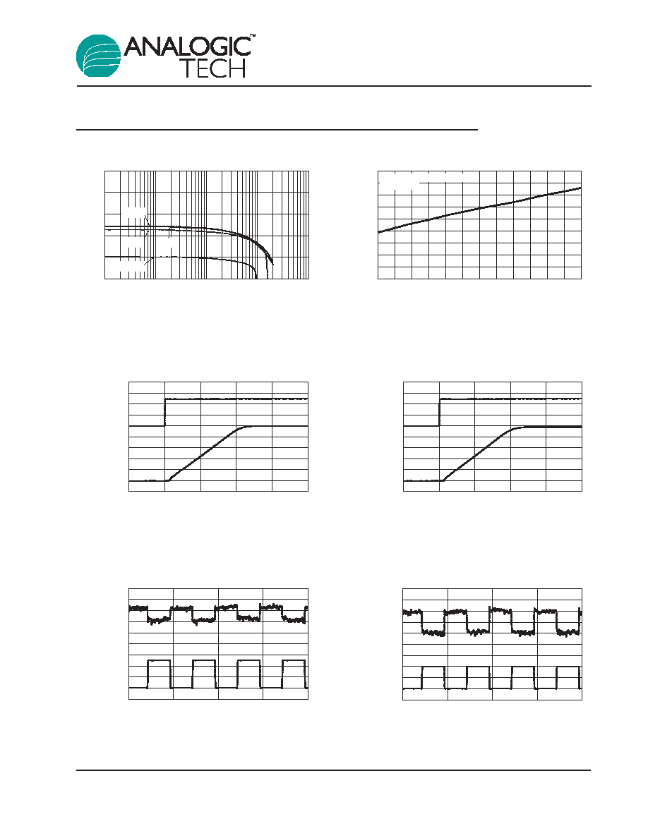
Typical Characteristics≠Flash Driver Charge Pump Section
Load Response vs. Time
(100mA Load)
Time (5ms/div)
V
OUT_FL
(10mV/div)
I
OUT
(50mA/div)
V
IN
= 3.5V
Load Response vs. Time
(50mA Load)
Time (5ms/div)
V
OUT_FL
(10mV/div)
I
OUT
(20mA/div)
V
IN
= 3.5V
Start-Up Time
(100mA Load)
TIme (100µs/div)
EN_FLSH
(1V/div)
V
OUT_FL
(1V/div)
Start-Up Time
(50mA Load)
EN_FLSH
(1V/div)
V
OUT_FL
(1V/div)
TIme (100µs/div)
Maximum Current Pulse vs. Supply Voltage
(V
OUT_FL
= 4.5V; EN_FL = V
IN
; EN/SET = GND)
Supply Voltage (V)
Maximum Current Pulse (mA)
0
50
100
150
200
250
300
350
400
450
3.0
3.1
3.2
3.3
3.4
3.5
3.6
3.7
3.8
3.9
4.0
4.1
4.2
One-shot pulse duration = 250ms
V
OUT
> 4.0V
Output Voltage vs. Output Current
(V
OUT_FL
= 4.5V; EN_FL = V
IN
; EN/SET = GND)
Output Current (mA)
Output Voltage (V)
4.40
4.44
4.48
4.52
4.56
4.60
0.1
1.0
10.0
100.0
1000.0
3.6V
3.0V
3.3V
2.7V
AAT2805
Dual High Efficiency Charge Pump
for White LED and Flash Applications
2805.2006.04.1.7
5

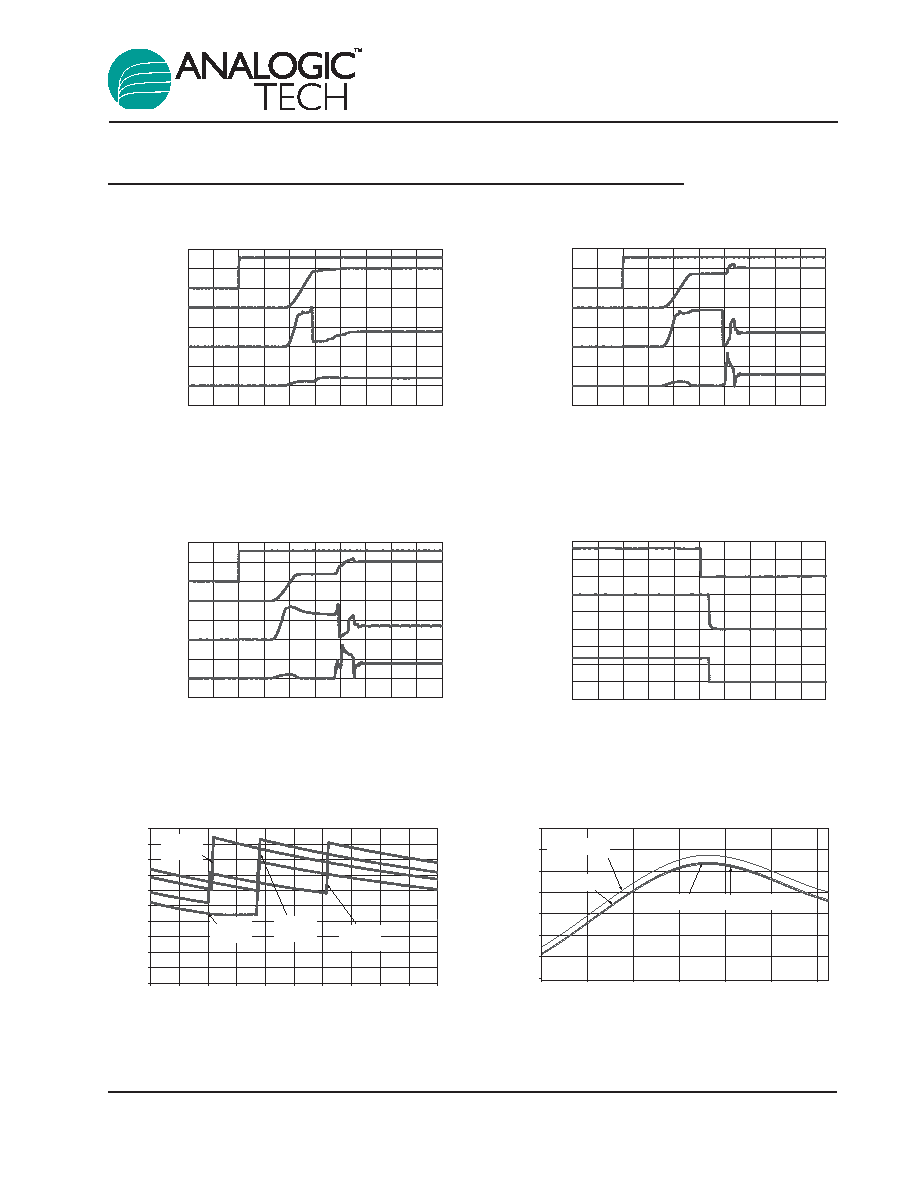
Typical Characteristics≠Flash Driver Charge Pump Section
Oscillator Frequency vs. Supply Voltage
Supply Voltage (V)
Oscillator Frequency (MHz)
1.10
1.15
1.20
1.25
1.30
2.7
3.2
3.7
4.2
4.7
-40∞C
+85∞C
+25∞C
Supply Current vs. Supply Voltage
Supply Voltage (V)
Supply Current (mA)
1.00
1.25
1.50
1.75
2.00
2.25
2.50
2.75
3.00
2.5
3.0
3.5
4.0
4.5
5.0
I
OUT
= 0A
C
3
= 1F
V
EN_FL
= V
IN
Output Ripple Voltage vs. Time
(I
OUT
= 100mA @ V
IN
= 3.5V)
Time (500ns/div)
I
IN
(10mA/div)
V
OUT
(20mV/div)
V
IN
(10mV/div)
Output Ripple Voltage vs. Time
(I
OUT
= 50mA @ V
IN
= 3.5V)
Time (500ns/div)
I
IN
(10mA/div)
V
OUT
(10mV/div)
V
IN
(10mV/div)
AAT2805
Dual High Efficiency Charge Pump
for White LED and Flash Applications
6
2805.2006.04.1.7
Typical Characteristics≠White LED Backlight Driver Section
Current Matching vs. Temperature
Temperature (
∞
∞C)
Current (mA)
19.0
19.2
19.4
19.6
19.8
20.0
20.2
20.4
-40
-20
0
20
40
60
80
Channel 2
Channel 3
Channel 1
Channel 4
Efficiency vs. Supply Voltage
Supply Voltage (V)
Efficiency (%)
0
10
20
30
40
50
60
70
80
90
100
2.6
2.8
2.9
3.1
3.2
3.4
3.6
3.7
3.9
4.0
4.2
4.1mA
V
F
= 2.9V
1mA
V
F
= 2.7V
10.2mA
V
F
= 3.1V
20mA
V
F
= 3.4V
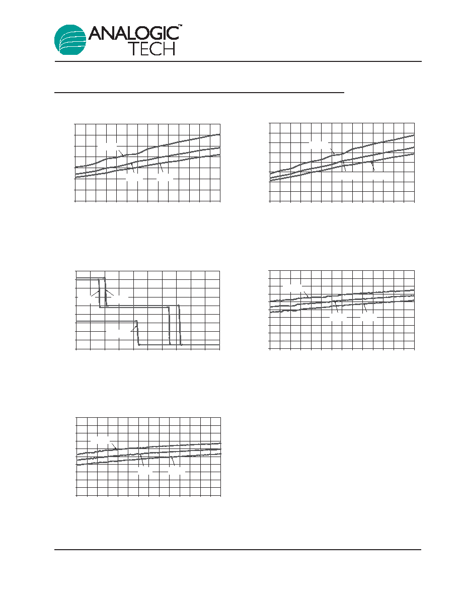
Turn-Off from 1.5X Mode
(V
IN
= 3.5V; 20mA Load)
Time (500µs/div)
EN
(2V/div)
I
IN
(100mA/div)
V
F
(1V/div)
Turn-On to 2X Mode
(V
IN
= 2.8V; 20mA Load)
Time (100µs/div)
EN
(2V/div)
CP
(2V/div)
I
IN
(200mA/div)
V
SINK
(500mV/div)
Turn-On to 1.5X Mode
(V
IN
= 3.5V; 20mA Load)
Time (100µs/div)
EN
(2V/div)
CP
(2V/div)
I
IN
(200mA/div)
V
SINK
(500mV/div)
Turn-On to 1X Mode
(V
IN
= 4.2V; 20mA Load)
Time (100µs/div)
EN
(2V/div)
CP
(2V/div)
I
IN
(200mA/div)
V
SINK
(500mV/div)
AAT2805
Dual High Efficiency Charge Pump
for White LED and Flash Applications
2805.2006.04.1.7
7
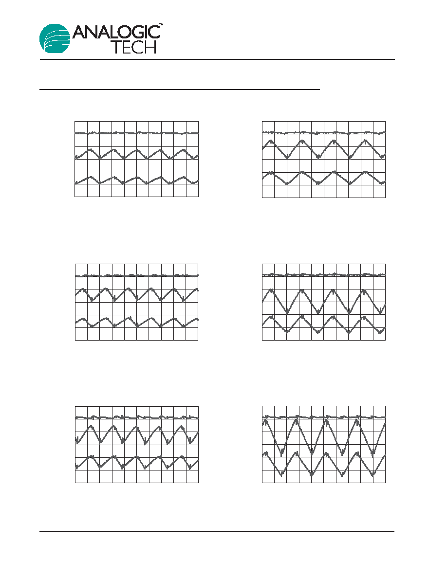
Typical Characteristics≠White LED Backlight Driver Section
Load Characteristics
(V
IN
= 3.2V; 2X Mode; 30mA Load)
Time (500ns/div)
V
IN
(40mV/div)
V
SINK
(40mV/div)
CP
(40mV/div)
Load Characteristics
(V
IN
= 4.2V; 1.5X Mode; 30mA Load)
Time (500ns/div)
V
IN
(40mV/div)
V
SINK
(40mV/div)
CP
(40mV/div)
Load Characteristics
(V
IN
= 2.9V; 2X Mode; 20mA Load)
Time (500ns/div)
V
IN
(40mV/div)
V
SINK
(40mV/div)
CP
(40mV/div)
Load Characteristics
(V
IN
= 3.9V; 1.5X Mode; 20mA Load)
Time (500ns/div)
V
IN
(40mV/div)
V
SINK
(40mV/div)
CP
(40mV/div)
Load Characteristics
(V
IN
= 2.7V; 2X Mode; 15mA Load)
Time (500ns/div)
V
IN
(40mV/div)
V
SINK
(40mV/div)
CP
(40mV/div)
Load Characteristics
(V
IN
= 3.7V; 1.5X Mode; 15mA Load)
Time (500ns/div)
V
IN
(40mV/div)
V
SINK
(40mV/div)
CP
(40mV/div)
AAT2805
Dual High Efficiency Charge Pump
for White LED and Flash Applications
8
2805.2006.04.1.7
Typical Characteristics≠White LED Backlight Driver Section
Enable Threshold Low vs. Input Voltage
Input Voltage (V)
Enable Threshold Low (V)
0.2
0.3
0.4
0.5
0.6
0.7
0.8
0.9
1
1.1
1.2
2.7 2.9 3.1 3.3 3.5 3.7 3.9 4.1 4.3 4.5 4.7 4.9 5.1 5.3 5.5
-40∞C
25∞C
85∞C
Enable Threshold High vs. Input Voltage
Input Voltage (V)
Enable Threshold High (V)
0.2
0.3
0.4
0.5
0.6
0.7
0.8
0.9
1
1.1
1.2
2.7 2.9 3.1 3.3 3.5 3.7 3.9 4.1 4.3 4.5 4.7 4.9 5.1 5.3 5.5
-40∞C
25∞C
85∞C
Input Ripple vs. Input Voltage
Input Voltage (V)
Amplitude (mV)
0
2
4
6
8
10
12
14
16
18
2.50 2.67 2.84 3.01 3.18 3.35 3.52 3.69 3.86 4.03 4.20
10.2mA
20mA
30mA
EN/SET Off Timeout vs. Input Voltage
Input Voltage (V)
EN/SET Off Timeout (
s)
0
50
100
150
200
250
300
350
400
2.7 2.9 3.1 3.3 3.5 3.7 3.9 4.1 4.3 4.5 4.7 4.9 5.1 5.3 5.5
-40∞C
25∞C
85∞C
EN/SET Latch Timeout vs. Input Voltage
Input Voltage (V)
EN/SET Latch Timeout (
s)
0
50
100
150
200
250
300
350
2.7 2.9 3.1 3.3 3.5 3.7 3.9 4.1 4.3 4.5 4.7 4.9 5.1 5.3 5.5
-40∞C
25∞C
85∞C
AAT2805
Dual High Efficiency Charge Pump
for White LED and Flash Applications
2805.2006.04.1.7
9
AAT2805
Dual High Efficiency Charge Pump
for White LED and Flash Applications
10
2805.2006.04.1.7
Functional Block Diagram
1X
1.5X
2X
Charge
Pump
Soft-Start
Control
1MHz
Oscillator
Voltage
Reference
C1+
C1-
C2+
C2-
D1
D2
D3
D4
GND
EN/SET
D/A
D/A
D/A
D/A
V
REF
Soft-Start
1MHz
Oscillator
2X Charge
Pump
C3
+
C3
-
EN_FLSH
V
OUT_FLSH
V
OUT_BL
6 X 16 Bit
ROM
6 X 16 Bit
ROM
Control
Logic
V
IN
Functional Description
The AAT2805 is a dual charge pump designed for
flash and white LED applications. The backlight
charge pump is a tri-mode load switch (1X) and high
efficiency (1.5X or 2X) charge pump device. To max-
imize power conversion efficiency, an internal sens-
ing circuit monitors the voltage required on each con-
stant current sink input and sets the load switch and
charge pump modes based on the input battery volt-
age and the current sink input voltage. As the battery
voltage discharges over time, the white LED charge
pump is enabled when any of the four current sink
inputs near dropout. The charge pump initially starts
in 1.5X mode. If the charge pump output drops
enough for any current source output to become
close to dropout, the charge pump will automatically
transition to 2X mode. The four constant current sink
inputs D1 to D4 can drive four individual LEDs with a
maximum current of 30mA per LED. The unused sink
inputs must be connected to V
OUT_BL
; otherwise, the
part will operate only in 2X charge pump mode. The
AS
2
Cwire serial interface enables and sets the con-
stant current sink magnitudes. AS
2
Cwire addressing
allows the LED main channels D1-D3 to be con-
trolled independently from the LED sub-channel D4.
The flash charge pump is a charge pump doubler
with regulated output voltage. It is designed to deliv-
er 120mA of continuous current and 250mA of
pulsed current.

The AAT2805 requires six external components:
three 1µF ceramic capacitors for the charge pump
flying capacitors (C
1
, C
2
, and C
3
), one 1µF ceramic
input capacitor (C
IN
), one 0.33µF to 1µF ceramic
capacitor for backlight charge pump output capacitor
(C
OUT
), and one 1µF ceramic capacitor for flash
charge pump output capacitor (C
OUT
).
Constant Current Output Level Settings
The constant current level for the LED channels is set
via the AS
2
Cwire serial interface according to a loga-
rithmic scale. The current level spacing is 1dB
between adjacent constant current settings. In this
manner, LED brightness appears to change linearly
when the settings are traversed. Because the inputs
D1 to D4 are true independent constant current
sinks, the voltage observed on any single given input
will be determined by the difference between V
OUT
and the actual forward voltage (V
F
) of the LED being
driven.
Since the constant current levels are programmable,
no PWM (pulse width modulation) or additional con-
trol circuitry is needed to control LED brightness.
This feature greatly reduces the burden on a micro-
controller or system IC to manage LED or display
brightness, allowing the user to "set it and forget it."
With its high-speed serial interface (>1MHz data
rate), the LED current drive can be changed suc-
cessively to brighten or dim LEDs, in smooth transi-
tions (e.g., to fade-out) or in abrupt steps, giving the
user complete programmability and real-time control
of LED brightness.
For each Max Current scale (see Table 1), there are
16 current level settings separated from one another
by approximately 1dB. Code 1 is full-scale current
and Code 15 is full-scale current attenuated by
roughly 14dB. Code 16 is reserved as a "no current"
setting. When programming the charge pump, it will
default to the 20mA maximum scale.
The AAT2805 offers an additional Low Current mode
with reduced quiescent current (see Table 2). This
mode is especially useful for low-current applications
where a continuous, low-current state is maintained.
The reduction in quiescent current significantly
reduces the impact due to maintaining a continuous
backlighting state.
Table 1: Constant Current Programming Levels.
Table 2: Low Current Register Settings.
Data
D1-D3 (mA)
D4 (mA)
1 0 0
2 0 0
3 0 0
4 0 0
5 0 0.05
6 0 0.5
7 0 1
8 0 2
9 0.05 0
10 0.5 0
11 1 0
12 2 0
13 0.05 0.05
14 0.5 0.5
15 1 1
16 2 2
Max I
OUT
(mA)
Data
20mA
30mA
15mA
1 20.0 30.0 15.0
2 17.8 26.7 13.3
3 15.9 23.8 11.9
4 14.3 21.4 10.7
5 12.7 19.0 9.5
6 11.1 16.7 8.3
7 10.2 15.2 7.6
8 8.9 13.3 6.7
9 7.9 11.9 6.0
10 7.0 10.5 5.2
11 6.3 9.5 4.8
12 5.7 8.6 4.3
13 5.1 7.6 3.8
14 4.4 6.7 3.3
15 4.1 6.2 3.1
16 0.0 0.0 0.0
AAT2805
Dual High Efficiency Charge Pump
for White LED and Flash Applications
2805.2006.04.1.7
11

AAT2805
Dual High Efficiency Charge Pump
for White LED and Flash Applications
12
2805.2006.04.1.7
AS
2
Cwire Serial Interface
The AS
2
Cwire single wire interface is used to set the
possible combinations of current levels and LED
channel states. AS
2
Cwire has addressing capability
for multiple data registers. With multiple data regis-
ters, the main and sub-channel can be programmed
together or independently from one another.
AS
2
Cwire relies on the number of rising edges of the
EN/SET pin to address and load the registers.
AS
2
Cwire latches data or address after the EN/SET
pin has been held high for time T
LAT
. Address or data
is differentiated by the number of EN/SET rising
edges. Since the data registers are 4 bits each, the
differentiating number of pulses is 2
4
or 16, so that
Address 1 is signified by 17 rising edges, Address 2
by 18 rising edges, and so forth. Data is set to any
number of rising edges between 1 and including 16.
A typical write protocol is a burst of EN/SET rising
edges, signifying a particular address, followed by a
pause with EN/SET held high for the T
LAT
timeout
period, a burst of rising edges signifying data, and a
T
LAT
timeout for the data registers. Once an address
is set, then multiple writes to the corresponding data
register are allowed.
When EN/SET is held low for an amount of time
greater than T
OFF
, the charge pump enters into shut-
down mode and draws less than 1µA from the sup-
ply. Address 1 is the default address on the first ris-
ing edge after the charge pump has been disabled.
Whenever shutdown mode is entered, all registers
are reset to 1.
AS
2
Cwire Addressing
Five addresses are available to enable all of the
part's functionality (see Table 3). Two 4-bit registers
control the main and sub-channel, giving 16 settings
for each. The main and sub-channel are pro-
grammed to the same constant current level by using
Address 1. Use Addresses 2 and 3 to program the
main and sub-channel independently. Use Address 4
to program the Max Current register, which sets the
Max Current scale. Lastly, Address 5 programs the
Low Current register. The Low Current register con-
trols the efficient Low Current mode.
When the Max Current register is programmed to 1,
2, or 3, changing the data for Addresses 1-3 will
result in the corresponding values found in Table 1.
When the Max Current register is programmed to 4,
the part is programmed to operate in Low Current
mode and the Data for Addresses 1-3 is irrelevant. In
Low Current mode, the Low Current register takes
precedence. See the Low Current Register Settings
table below for the current level settings and main/
sub-configurations that result.
Table 3: Address Settings.
Max Current and Low Current Registers
Use the Max Current and Low Current registers to
program constant current settings outside of the
20mA Max scale. By default (without changing the
Max Current register), the charge pump operates in
the 20mA Max scale (see Table 1). For example, to
change to the 30mA Max scale, address the Max
Current register with 20 rising edges and pause for
T
LAT
. Program the Max Current register with 2 rising
edges and pause for T
LAT
. The part will next operate
in the same Data row, but for the setting found in the
30mA Max column. Next, to change to a different
setting on the 30mA Max scale, address the D1-D4
register with 17 rising edges. Program the new con-
stant current level with 1-16 rising edges. The part will
update to the new Data setting as shown in Table 1.
The charge pump has a distinct Low Current mode
with ultra-low quiescent current. For drive currents of
2mA or less, the part operates with significantly
reduced quiescent current. This is particularly useful
for applications requiring an "always on" condition
such as transmissive displays. For another example,
to change to Low Current mode, address the Max
Current register with 20 rising edges and pause for
T
LAT
. Program the Max Current register with 4 rising
edges and pause for
TLAT
. Address the Low Current
register with 21 rising edges and pause for T
LAT
.
Program the Low Current register with 1-16 rising
edges. The part will update to the new Low Current
mode setting and operate with significantly reduced
quiescent current.
EN/SET Addressed
Address
Edges
Register
1
17
1&2: D1-D4 Current
2
18
1: D1-D3 Current
3
19
2: D4 Current
4
20
3: Max Current
5
21
4: Low Current
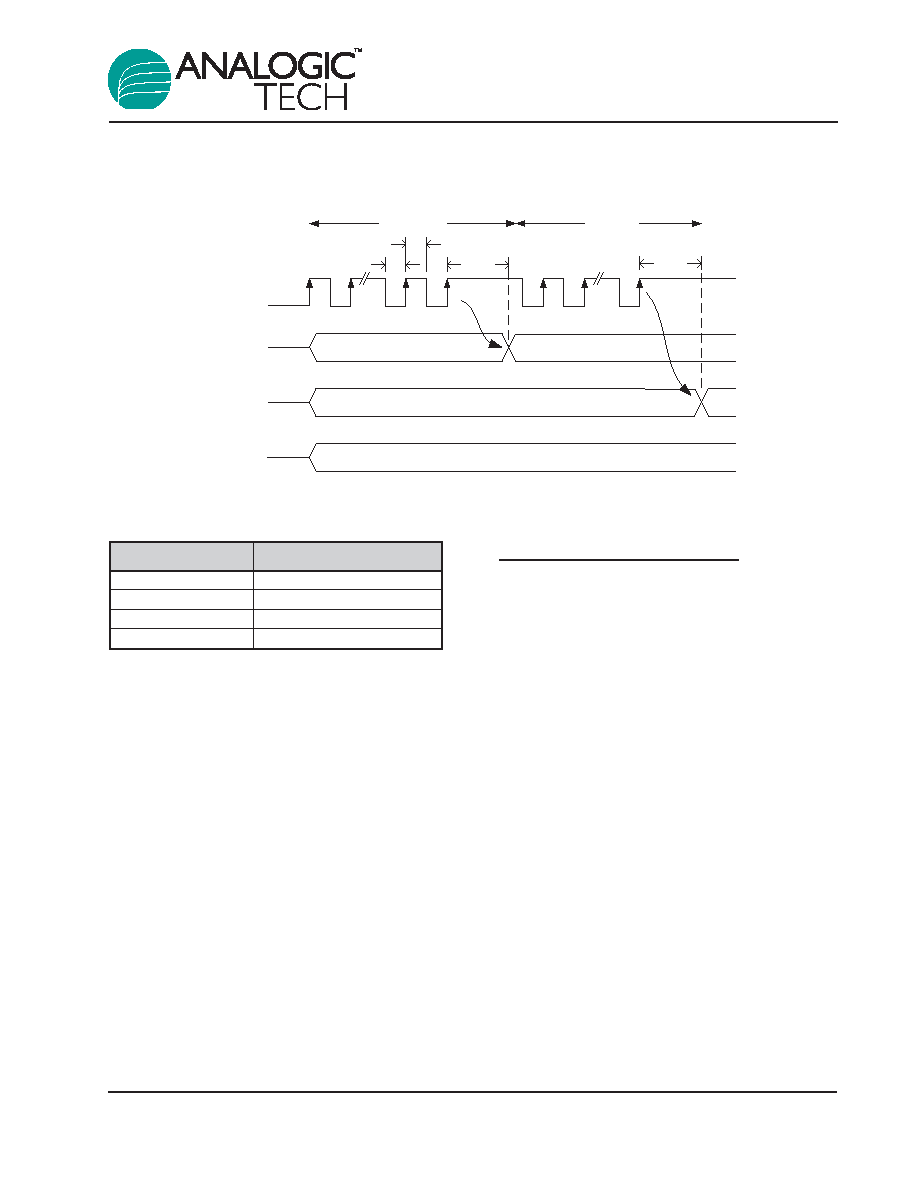
Table 4: Maximum Current Settings Address 4.
Disabled Current Sinks
The backlight charge pump is equipped with an auto-
disable feature to protect against an LED failure con-
dition. Current sink inputs that are not used should
be disabled. To disable and properly terminate
unused current sink inputs, they must be tied to V
OUT
.
If left unconnected or terminated to ground, the part
will be forced to operate in 2X charge pump mode.
Properly terminating unused current sink inputs is
important to prevent the charge pump modes from
activating prematurely. When properly terminated,
only a small sense current flows for each disabled
channel. The sense current for each disabled chan-
nel is less than 120µA.
Applications Information
LED Selection
The AAT2805 is specifically intended for driving white
LEDs. However, the device design will allow the
AAT2805 to drive most types of LEDs with forward
voltage specifications ranging from 2.0V to 4.3V.
LED applications may include main display back-
lighting, camera photo-flash applications, color
(RGB) LEDs, infrared (IR) diodes for remotes, and
other loads benefiting from a controlled output cur-
rent generated from a varying input voltage. Since
the D1 to D4 input current sinks are matched with
negligible voltage dependence, the LED brightness
will be matched regardless of the specific LED for-
ward voltage (V
F
) levels.
In some instances (e.g., in high-luminous-output
applications such as photo flash), it may be neces-
sary to drive high-V
F
type LEDs. The low dropout cur-
rent sinks in the AAT2805 make it capable of driving
LEDs with forward voltages as high as 4.3V at full
current from an input supply as low as 3.0V. Outputs
can be paralleled to drive high-current LEDs without
complication.
Data Max
Current
1 20mA Max
Scale
2 30mA Max
Scale
3 15mA Max
Scale
4
Low Current Mode
AAT2805
Dual High Efficiency Charge Pump
for White LED and Flash Applications
2805.2006.04.1.7
13
AS
2
Cwire Serial Interface Timing Diagram
Address
Data
1
EN/SET
2
17
18
Address
Data Reg 1
Data Reg 2
1
2 . . .
n <= 16
0
1
0
0
n
T
HI
T
LO
T
LAT
T
LAT

AAT2805
Dual High Efficiency Charge Pump
for White LED and Flash Applications
14
2805.2006.04.1.7
Device Switching Noise Performance
The AAT2805 operates at a fixed frequency of
approximately 1MHz to control noise and limit har-
monics that can interfere with the RF operation of cel-
lular telephone handsets or other communication
devices. Back-injected noise appearing on the input
pin of the charge pump is 20mV peak-to-peak, typi-
cally ten times less than inductor-based DC/DC
boost converter white LED backlight solutions. The
AAT2805 soft-start feature prevents noise transient
effects associated with inrush currents during start-
up of the charge pump circuit.
Capacitor Selection
Careful selection of the six external capacitors C
IN
,
C
1
, C
2
, C
3
and C
OUT
(for backlight and flash) is impor-
tant because they will affect turn-on time, output rip-
ple, and transient performance. Optimum perform-
ance will be obtained when low equivalent series
resistance (ESR) (<100m
) ceramic capacitors are
used. In general, low ESR may be defined as less
than 100m
. A value of 1µF for all six capacitors is
a good starting point when choosing capacitors.
Capacitor Characteristics
Ceramic composition capacitors are highly recom-
mended over all other types of capacitors for use with
the AAT2805. Ceramic capacitors offer many advan-
tages over their tantalum and aluminum electrolytic
counterparts. A ceramic capacitor typically has very
low ESR, is lowest cost, has a smaller PCB footprint,
and is non-polarized. Low ESR ceramic capacitors
help maximize charge pump transient response.
Since ceramic capacitors are non-polarized, they are
not prone to incorrect connection damage.
Equivalent Series Resistance
ESR is an important characteristic to consider when
selecting a capacitor. ESR is a resistance internal to
a capacitor that is caused by the leads, internal con-
nections, size or area, material composition, and
ambient temperature. Capacitor ESR is typically
measured in milliohms for ceramic capacitors and
can range to more than several ohms for tantalum or
aluminum electrolytic capacitors.
Ceramic Capacitor Materials
Ceramic capacitors less than 0.1µF are typically
made from NPO or C0G materials. NPO and C0G
materials generally have tight tolerance and are
very stable over temperature. Larger capacitor val-
ues are usually composed of X7R, X5R, Z5U, or
Y5V dielectric materials. Large ceramic capacitors
(i.e., greater than 2.2µF) are often available in low-
cost Y5V and Z5U dielectrics, but capacitors
greater than 1µF are not typically required for
AAT2805 applications.
Capacitor area is another contributor to ESR.
Capacitors that are physically large will have a lower
ESR when compared to an equivalent material small-
er capacitor. These larger devices can improve cir-
cuit transient response when compared to an equal
value capacitor in a smaller package size.
Thermal Protection
The AAT2805 has a thermal protection circuit that
will shut down the two charge pumps if the die tem-
perature rises above the thermal limit.
Charge Pump Power Efficiency
Backlight Charge Pump: The charge pump effi-
ciency discussion in the following sections only
accounts for the efficiency of the charge pump sec-
tion itself. Due to the unique circuit architecture, it
is very difficult to measure efficiency in terms of a
percent value comparing input power over output
power. Since the outputs are pure constant current
sinks and typically drive individual loads, it is diffi-
cult to measure the output voltage for a given out-
put (D1 to D4) to derive an overall output power
measurement. For any given application, white
LED forward voltage levels can differ, yet the out-
put drive current will be maintained as a constant.
This makes quantifying output power a difficult task
when taken in the context of comparing to other white
LED driver circuit topologies. A better way to quantify
total device efficiency is to observe the total input
power to the device for a given LED current drive
level. The best white LED driver for a given applica-
tion should be based on trade-offs of size, external
component count, reliability, operating range, and
total energy usage...not just "% efficiency."

AAT2805
Dual High Efficiency Charge Pump
for White LED and Flash Applications
2805.2006.04.1.7
15
Efficiency of the AAT2805 may be quantified under
very specific conditions and is dependent upon the
input voltage versus the output voltage seen across
the loads applied to outputs D1 through D4 for a given
constant current setting. Depending on the combina-
tion of V
IN
and voltages sensed at the current sinks,
the device will operate in load switch mode. When
any one of the voltages sensed at the current sinks
nears dropout, the device will operate in 1.5X or 2X
charge pump mode. Each of these modes will yield
different efficiency values. Refer to the following two
sections for explanations for each operational mode.
Load Switch Mode Efficiency: The load switch
mode is operational at all times and functions alone
to enhance device power conversion efficiency when
V
IN
is greater than the voltage across the load. When
in load switch mode, the voltage conversion efficien-
cy is defined as output power divided by input power:
The expression to define the ideal efficiency (
) can
be rewritten as:
-or-
Charge Pump Mode Efficiency: Fractional charge
pumps will boost the input supply voltage in the event
where V
IN
is less than the voltage required on the con-
stant current source outputs. The efficiency (
) can be
simply defined as a linear voltage regulator with an
effective output voltage that is equal to one and a half
or two times the input voltage. Efficiency (
) for an
ideal 1.5X charge pump can typically be expressed
as the output power divided by the input power:
In addition, with an ideal 1.5X charge pump, the out-
put current may be expressed as 2/3 of the input cur-
rent. The expression to define the ideal efficiency (
)
can be rewritten as:
-or-
For a charge pump with an output of 5V and a nom-
inal input of 3.5V, the theoretical efficiency is 95%.
Due to internal switching losses and IC quiescent
current consumption, the actual efficiency can be
measured at 93%. These figures are in close agree-
ment for output load conditions from 1mA to 100mA.
Efficiency will decrease as load current drops below
0.05mA or when level of V
IN
approaches V
OUT
.
Flash Charge Pump: The flash charge pump is a
regulated output voltage doubling charge pump. The
efficiency is defined as a linear voltage regulator with
an effective output voltage that is equal to two times
the input voltage. The expression to define the ideal
efficiency can be written as:
-or-
For a charge pump with an output of 5V and a nom-
inal input of 3V, the theoretical efficiency is 83.3%.
Due to internal switching losses and IC quiescent
current consumption, the actual efficiency can be
measured at approximately 82%. Efficiency will
decrease as the level of V
IN
approaches that of the
regulated V
OUT
. Refer to the device typical charac-
teristics curves for expected actual efficiency
based on either input voltage or load current.
(%) = 100
V
OUT
2.0V
IN
= P
OUT
= V
OUT
◊ I
OUT
= V
OUT
P
IN
V
IN
◊ 2.0I
OUT
2.0V
IN
(%) = 100
V
OUT
1.5V
IN
= P
OUT
= V
OUT
◊ I
OUT
= V
OUT
P
IN
V
IN
◊ 1.5I
OUT
1.5V
IN
=
P
OUT
P
IN
(%) = 100
V
OUT
V
IN
= P
OUT
= V
OUT
◊ I
OUT
= V
OUT
P
IN
V
IN
◊ I
OUT
V
IN
=
P
OUT
P
IN

AAT2805
Dual High Efficiency Charge Pump
for White LED and Flash Applications
16
2805.2006.04.1.7
Advanced Analogic Technologies, Inc.
830 E. Arques Avenue, Sunnyvale, CA 94085
Phone (408) 737-4600
Fax (408) 737-4611
Ordering Information
Package Information
TDFN44-16
All dimensions in millimeters.
Index Area
(D/2 x E/2)
Detail "A"
Detail "B"
Top View
Bottom View
Detail "A"
Side View
Option A:
C0.30 (4x) max
Chamfered corner
Option B:
R0.30 (4x) max
Round corner
Detail "B"
0.16
Pin 1 Indicator
(optional)
0.1 REF
4.00 ± 0.05
2.60 ± 0.05
4.00
±
0.05
3.30
±
0.05
0.8
+
0.05 -0.20
0.05 ± 0.05
0.229
±
0.051
7.5∞ ± 7.5∞
0.375 ± 0.125
0.3 ± 0.10
0.45
±
0.05
0.23
±
0.05
0.075 ± 0.075
All AnalogicTech products are offered in Pb-free packaging. The term "Pb-free" means
semiconductor products that are in compliance with current RoHS standards, including
the requirement that lead not exceed 0.1% by weight in homogeneous materials. For more
information, please visit our website at http://www.analogictech.com/pbfree.
Package
Marking
1
Part Number (Tape and Reel)
2
TDFN44-16
NIXYY
AAT2805IXN-4.5-T1
1. XYY = assembly and date code.
2. Sample stock is generally held on part numbers listed in BOLD.
© Advanced Analogic Technologies, Inc.
AnalogicTech cannot assume responsibility for use of any circuitry other than circuitry entirely embodied in an AnalogicTech product. No circuit patent licenses, copyrights, mask work rights,
or other intellectual property rights are implied. AnalogicTech reserves the right to make changes to their products or specifications or to discontinue any product or service without notice.
Customers are advised to obtain the latest version of relevant information to verify, before placing orders, that information being relied on is current and complete. All products are sold sub-
ject to the terms and conditions of sale supplied at the time of order acknowledgement, including those pertaining to warranty, patent infringement, and limitation of liability. AnalogicTech
warrants performance of its semiconductor products to the specifications applicable at the time of sale in accordance with AnalogicTech's standard warranty. Testing and other quality con-
trol techniques are utilized to the extent AnalogicTech deems necessary to support this warranty. Specific testing of all parameters of each device is not necessarily performed.
AnalogicTech and the AnalogicTech logo are trademarks of Advanced Analogic Technologies Incorporated. All other brand and product names appearing in this document are regis-
tered trademarks or trademarks of their respective holders.