AAT3113/13A, AAT3114/14A
High Efficiency 1.5X Fractional Charge
Pumps For White LED Applications
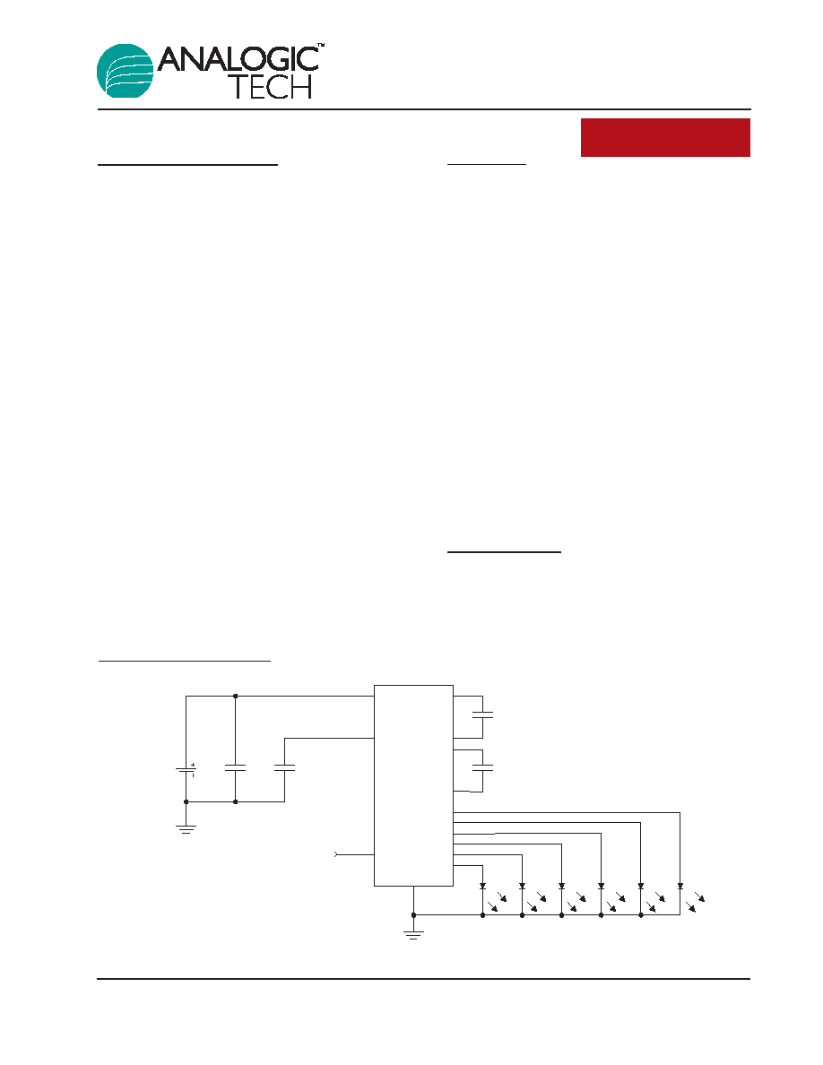
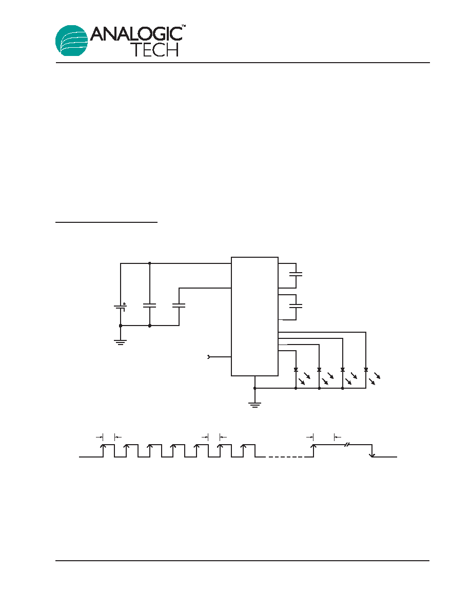
Typical Application
C
IN
1
µ
F
V
BATTERY
C
OUT
1
µ
F
EN/SET
C1
1
µ
F
C2
1
µ
F
D4
D3
D2
D1
VIN
VOUT
C1+
C1-
C2+
C2-
D1
D2
D3
D4
EN/SET
GND
AAT3114/14A
D5
D6
D5
D6
3113.2005.11.1.8
1
ChargePump
TM
General Description
The AAT3113/13A and AAT3114/14A are low noise,
constant frequency charge pump DC/DC converters
that use fractional (1.5X) conversion to increase effi-
ciency in white LED applications. The devices can
be used to produce current levels up to 20mA for
each output from a 2.7V to 5.5V input. A low exter-
nal parts count (two 1µF flying capacitors and two
small bypass capacitors at V
IN
and OUT) makes
these devices ideally suited for small battery-pow-
ered applications.
AnalogicTech's Simple Serial ControlTM (S
2
CwireTM)
interface is used to enable, disable, and set the
LED drive current for 32-level logarithmic scale LED
brightness control. AAT3113/13A and AAT3114/14A
devices have a thermal management system for
protection in the event of a short-circuit condition on
any of the output pins. Built-in soft-start circuitry
prevents excessive inrush current during start-up.
A high switching frequency enables the use of small
external capacitors. A low-current shutdown feature
disconnects the load from V
IN
and reduces quies-
cent current to less than 1µA. The AAT3113/13A
provides four LED current source outputs, and the
AAT3114/14A provides six. The AAT3113/13A is
available in the Pb-free 12-pin TSOPJW package,
and the AAT3114/14A is available in the Pb-free 16-
pin QFN package.
Features
∑
AAT3113/13A: Four Outputs
∑
AAT3114/14A: Six Outputs
∑
20mA Full-Scale Current
∑
32-Position Logarithmic Scale with Digital
Control
∑
Simple Serial Control (S
2
Cwire) Interface
∑
Low Noise Constant Frequency Operation
∑
33% Less Input Current Than Doubler
Charge Pump
∑
High Accuracy Brightness Matching
∑
Small Application Circuit
∑
Regulated Output Current
∑
Automatic Soft Start
∑
V
IN
Range: 2.7V to 5.5V
∑
No Inductors
∑
600kHz Switching Frequency
∑
I
Q
<1µA in Shutdown
∑
Temperature Range: -40∞C to 85∞C
∑
16-Pin QFN, 12-Pin TSOPJW Package
Applications
∑
Programmable Current Source
∑
White LED Backlighting
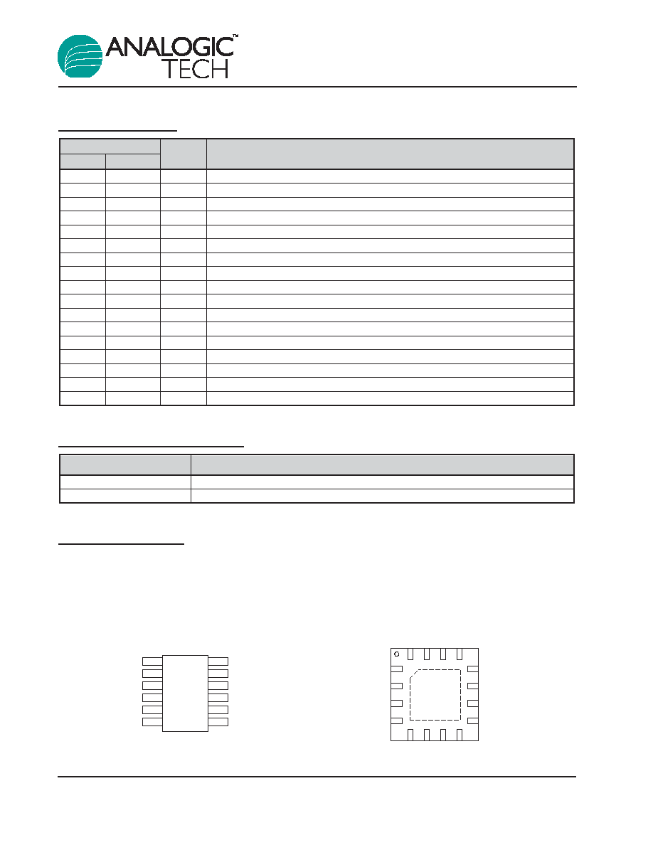
Pin Descriptions
Part Number Descriptions
Pin Configuration
TSOPJW-12
QFN44-16
(Top View)
(Top View)
AAT3113/13A
AAT3114/14A
1
2
3
4
12
11
10
9
5
6
7
8
16
15
14
13
D2
D3
D4
D5
D6
C1+
C1-
NC
OUT
C2+
C2-
GND
NC
VIN
EN/SET
D1
1
2
3
4
5
6
12
11
10
9
8
7
C2+
OUT
C1-
C1+
D4
D3
C2-
GND
VIN
EN/SET
D1
D2
Part Number
Function
AAT3113-20, AAT3113A-20
Four diode outputs, 20mA full scale.
AAT3114-20, AAT3114A-20
Six diode outputs, 20mA full scale.
Pin #
QFN44-16 TSOPJW-12
Symbol Function
1
7
D2
Current source output.
2
6
D3
Current source output.
3
5
D4
Current source output.
4
N/A
D5
Current source output (AAT3114/14A option only).
5
N/A
D6
Current source output (AAT3114/14A option only).
6
4
C1+
Flying capacitor 1 positive terminal.
7
3
C1-
Flying capacitor 1 negative terminal.
8
N/A
NC
No connect.
9
2
OUT
Charge pump output. Requires 1µF bypass capacitor to ground.
10
1
C2+
Flying capacitor 2 positive terminal.
11
12
C2-
Flying capacitor 2 negative terminal.
12
11
GND
Ground.
13
N/A
NC
No connect.
14
10
VIN
Input power supply. Requires 1µF bypass capacitor to ground.
15
9
EN/SET
Control pin using S
2
Cwire serial interface.
16
8
D1
Current source output 1. Required reference current source. Do not leave pin floating.
EP
Exposed paddle (bottom); connect to GND directly beneath package.
AAT3113/13A, AAT3114/14A
High Efficiency 1.5X Fractional Charge
Pumps For White LED Applications
2
3113.2005.11.1.8

Absolute Maximum Ratings
T
A
= 25∞C, unless otherwise noted.
Electrical Characteristics
V
IN
= 3.5V, T
A
= -40∞C to +85∞C, unless otherwise noted. Typical values are at T
A
= 25∞C.
Symbol
Description
Conditions
Min Typ Max Units
Input Power Supply
V
IN
Operation Range
2.7
5.5
V
I
CC
Operating Current
Active, No Load Current
1
2
mA
I
SHDN
Shutdown Current
EN = 0
1
µA
I
DX
Output Current
AAT3113/13A: 3.0
V
IN
5.5 T
A
= 25∞C, All
18
20
22
mA
AAT3114/14A: 3.2
V
IN
5.5 Outputs Max Current
I
D
/
V
IN
Output Current Line
3.0
V
IN
5.5
-2
2
%/V
Regulation
Current Matching
I
(D-Match)
Between Any
VD1:Dn = 3.6, V
IN
= 3.3V
0.3
%
Two Outputs
Efficiency
V
IN
= 3.5, I
OUT(total)
= 40mA
93
%
Charge Pump
t
SS
Soft-Start Time
400
µs
F
CLK
Clock Frequency
300
600 900
kHz
EN/SET
V
EN(L)
Enable Threshold Low
V
IN
= 2.7 to 5.5V
0.5
V
V
EN(H)
Enable Threshold High V
IN
= 2.7 to 5.5V
1.4
V
t
LO
EN/SET Low Time
0.3
75
µs
t
HI
Minimum EN/SET
50
ns
High Time
t
OFF
EN/SET Off Timeout
300 500
µs
Input Current EN/SET Input Leakage V
IN
= 5.5V
-1
1
µA
Symbol
Description
Value
Units
V
IN
Input Voltage
-0.3 to 6
V
V
OUT
Charge Pump Output
-0.3 to 6
V
V
EN/SET
EN/SET to GND Voltage
-0.3 to 6
V
V
EN/SET(MAX)
Maximum EN/SET to Input Voltage
0.3
V
I
OUT
Maximum DC Output Current (sum of I
OUT
and D currents)
150
mA
JA
Thermal Resistance
37
∞C/W
T
J
Operating Junction Temperature Range
-40 to 150
∞C
AAT3113/13A, AAT3114/14A
High Efficiency 1.5X Fractional Charge
Pumps For White LED Applications
3113.2005.11.1.8
3

Typical Characteristics
V
IN
= 3.5V, C
IN
= C
OUT
= C
1
= C
2
= 1µF, T
A
= 25∞C, unless otherwise noted.
Oscillator Frequency vs. Temperature
610
620
630
640
650
660
670
680
690
700
710
-40
-20
0
20
40
60
80
100
Temperature (
∞
C)
F
OSC
(kHz)
Shutdown Current vs. Temperature
0.001
0.010
0.100
1.000
-40
-20
0
20
40
60
80
100
Temperature (
∞
C)
Shutdown Current (
µ
A)
Efficiency vs. Load Current
80
82
84
86
88
90
92
94
96
0
20
40
60
80
100
120
Load Current (mA)
Efficiency (%)
Quiescent Current vs. Supply Voltage
0.6
0.7
0.8
0.9
1.0
1.1
1.2
3.0
3.5
4.0
4.5
5.0
5.5
Supply Voltage (V)
I
Q
(mA)
Efficiency vs. Supply Voltage
60
65
70
75
80
85
90
95
100
3.0
3.2
3.4
3.6
3.8
4.0
4.2
4.4
Supply Voltage (V)
Efficiency (%)
120mA
80mA
60mA
40mA
30mA
20mA
Quiescent Current vs. Temperature
0.860
0.880
0.900
0.920
0.940
0.960
0.980
1.000
-40
-20
0
20
40
60
80
100
Temperature (
∞
C)
I
Q
(mA)
AAT3113/13A, AAT3114/14A
High Efficiency 1.5X Fractional Charge
Pumps For White LED Applications
4
3113.2005.11.1.8
Typical Characteristics
V
IN
= 3.5V, C
IN
= C
OUT
= C
1
= C
2
= 1µF, T
A
= 25∞C, unless otherwise noted.
0.750
0.775
0.800
0.825
0.850
0.875
0.900
0.925
0.950
0.975
1.000
2.5
3.0
3.5
4.0
4.5
5.0
5.5
V
IN
(V)
V
IH
and V
IL
(V)
V
IH
V
IL
V
IH
and V
IL
vs. V
IN
I
DIODE
vs. V
DIODE
0
20
40
60
80
100
120
140
3.0
3.2
3.4
3.6
3.8
4.0
V
DIODE
(V)
I
DIODE
(mA)
I
DIODE
Response
(-9dB to -10dB)
Time (10µs/div)
ENSET
(2V/div)
I
DIODE
-9dB
0dB
-10dB
-31dB
I
DIODE
vs. V
IN
0
20
40
60
80
100
120
140
3.0
3.5
4.0
4.5
V
IN
(V)
I
DIODE
(mA)
I
DIODE
Response
(-31dB to 0dB)
Time (10µs/div)
ENSET
(2V/div)
I
DIODE
-31dB
0dB
Normalized I
DIODE
vs. Temperature
0.950
0.960
0.970
0.980
0.990
1.000
1.010
1.020
-40
-20
0
20
40
60
80
100
Temperature (
∞
C)
I
DIODE
AAT3113/13A, AAT3114/14A
High Efficiency 1.5X Fractional Charge
Pumps For White LED Applications
3113.2005.11.1.8
5

Typical Characteristics
V
IN
= 3.5V, C
IN
= C
OUT
= C
1
= C
2
= 1µF, T
A
= 25∞C, unless otherwise noted.
120mA Load Characteristics
Time (1µs/div)
20mV/div
IN
OUT
V
DIODE
80mA Load Characteristics
Time (1µs/div)
20mV/div
IN
OUT
V
DIODE
60mA Load Characteristics
Time (1µs/div)
20mV/div
IN
OUT
V
DIODE
40mA Load Characteristics
Time (1µs/div)
10mV/div
IN
OUT
V
DIODE
Turn-Off
Time (200µs/div)
ENSET
(2V/div)
OUT
(5V/div)
V
DIODE
(5V/div)
I
IN
(50mA/div)
Turn-On
Time (100µs/div)
ENSET
(2V/div)
OUT
(5V/div)
V
DIODE
(2V/div)
I
IN
(50mA/div)
AAT3113/13A, AAT3114/14A
High Efficiency 1.5X Fractional Charge
Pumps For White LED Applications
6
3113.2005.11.1.8

Functional Block Diagram
Voltage
Reference
Soft Start
600kHz
Oscillator
1.5X
Charge
Pump
S
2
Cwire
Interface
32x8 bit
ROM
Current
Mode
DAC
8
5
VIN
C1+
C1-
C2+
C2-
OUT
D1
D2
D3
D4
GND
* AAT3114/14A only
EN/SET
D5*
D6*
AAT3113/13A, AAT3114/14A
High Efficiency 1.5X Fractional Charge
Pumps For White LED Applications
3113.2005.11.1.8
7
Functional Description
The AAT3113/13A and AAT3114/14A devices are
high efficiency 1.5X fractional charge pumps
intended for white LED backlight applications. The
fractional charge pump consists of a linear regula-
tor followed by a 1.5X charge pump. The
AAT3113/13A and AAT3114/14A require only four
external components: two 1µF ceramic capacitors
for the charge pump flying capacitors (C1 and C2),
one 1µF ceramic capacitor for C
IN
, and one 0.33µF
to 1µF ceramic capacitor for C
OUT
. The charge
pump output is converted into four or six constant
current outputs (D1 to D4 or D6) to drive four or six
individual LEDs with a maximum of 20mA each.
The current source output magnitude is controlled
by the EN/SET serial data S
2
Cwire interface. The
interface records rising edges of the EN/SET pin
and decodes them into 32 individual current level
settings each 1dB apart (see Table 1, Current
Level Settings). Code 32 is full scale, and Code 1
is full scale attenuated by 31dB. The modulo 32
interface wraps states back to state 1 after the
32nd clock. With each EN/SET pulse, the output
current increases by 1dB. To decrease the output
current by 1dB, 31 EN/SET clock pulses are
required. The counter can be clocked at speeds up
to 1MHz, so intermediate states are not visible.
The first rising edge of EN/SET enables the IC and
initially sets the output LED current to -31dB, the
lowest setting equal to 525µA. Once the final clock
cycle is input for the desired brightness level, the
EN/SET pin is held high to maintain the device out-
put current at the programmed level. The device is
disabled 500µs after the EN/SET pin transitions to
a logic low state.

AAT3113/13A, AAT3114/14A
High Efficiency 1.5X Fractional Charge
Pumps For White LED Applications
8
3113.2005.11.1.8
Applications Information
Current Level Settings
LED current level is set via the serial interface
according to a logarithmic scale where each code
is 1dB greater than the previous code. In this man-
ner, the LED brightness appears linear with each
increasing code.
Table 1: Current Level Settings.
Code
20mA max
Code
20mA max
1
0.549
17
3.529
2
0.627
18
4.000
3
0.706
19
4.471
4
0.784
20
5.020
5
0.863
21
5.647
6
1.020
22
6.353
7
1.098
23
7.059
8
1.255
24
7.922
9
1.412
25
8.941
10
1.569
26
10.039
11
1.804
27
11.216
12
1.961
28
12.627
13
2.275
29
14.118
14
2.510
30
15.843
15
2.824
31
17.804
16
3.137
32
20.000
Normalized Current Level Settings
0.0
0.1
0.2
0.3
0.4
0.5
0.6
0.7
0.8
0.9
1.0
1
2
3
4
5
6
7
8
9
10 11 12 13 14 15 16 17 18 19 20 21 22 23 24 25 26 27 28 29 30 31 32
Code
Normalized Current to Full Scale
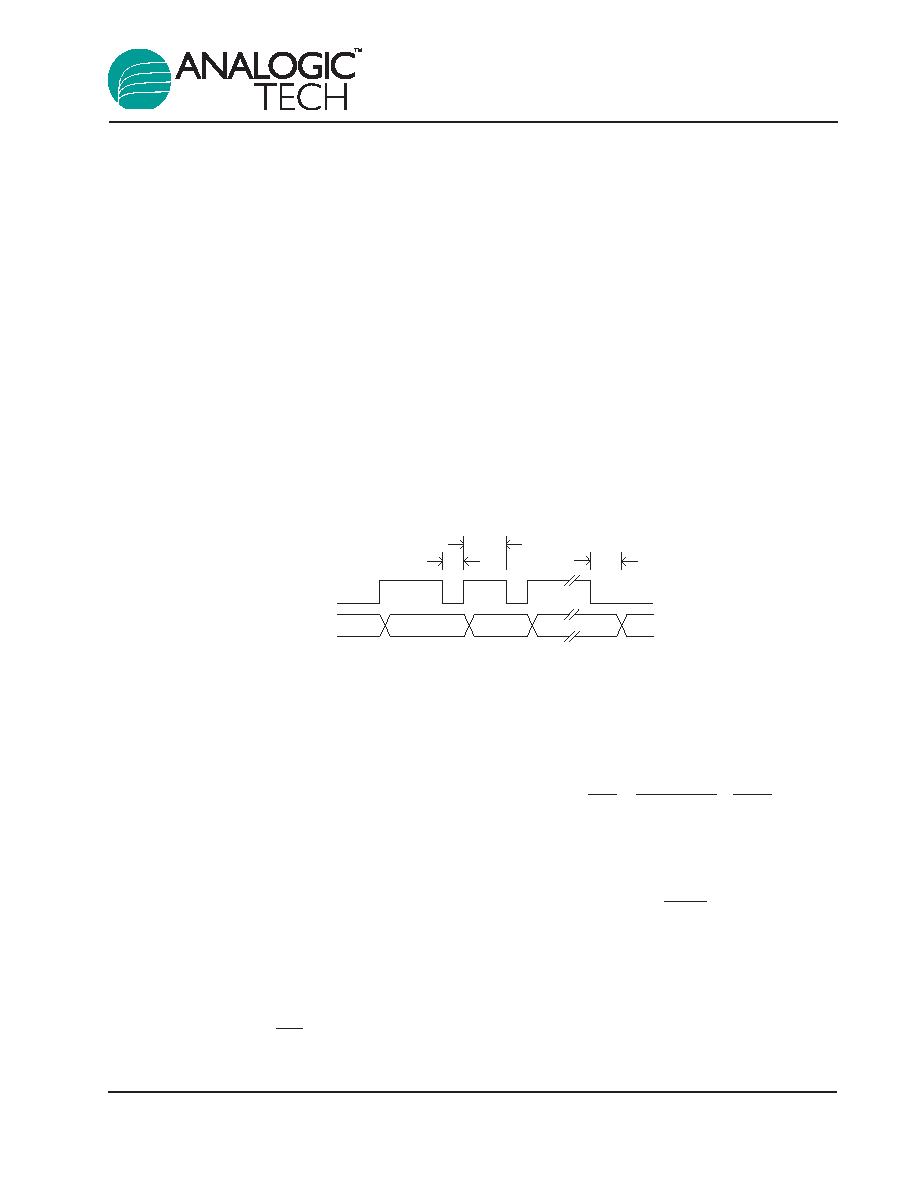
EN/SET Serial Interface
The current source output magnitude is controlled
by the EN/SET pin using AnalogicTech's Simple
Serial Control (S
2
Cwire) interface. The interface
records rising edges of the EN/SET pin and
decodes them into 32 individual current level set-
tings each 1dB apart. Code 32 is full scale, and
Code 1 is full scale attenuated by 31dB. The mod-
ulo 32 interface wraps states back to state 1 after
the 32nd clock, so 1dB of attenuation is achieved
by clocking the EN/SET pin 31 times (see graph
titled, "I
DIODE
Response -9dB to -10dB"). The
counter can be clocked at speeds up to 1MHz, so
intermediate states are not visible. The first rising
edge of EN/SET enables the IC and initially sets
the output LED current to -31dB, the lowest setting
equal to 525µA. Once the final clock cycle is input
for the desired brightness level, the EN/SET pin is
held high to maintain the device output current at
the programmed level. The device is disabled
500µs after the EN/SET pin transitions to a logic
low state.
The EN/SET timing is designed to accommodate a
wide range of data rates. After the first rising edge
of EN/SET, the charge pump is enabled and reach-
es full capacity after the soft-start time (T
SS
). During
the soft-start time, multiple clock pulses may be
entered on the EN/SET pin to set the final output
current level with a single burst of clocks.
Alternatively, the EN/SET clock pulses may be
entered one at a time to gradually increase the LED
brightness over any desired time period. A constant
current is sourced as long as EN/SET remains in a
logic high state. The current source outputs are
switched off after EN/SET has remained in a low
state for at least the t
OFF
timeout period.
LED Selection
AAT3113/13A and AAT3114/14A devices are
designed to drive white LEDs with forward voltages
of less than 4.2V. Since the D1:D6 output current
sources are matched with negligible voltage
dependence, the LED brightness will be matched
regardless of their forward voltage matching.
Charge Pump Efficiency
The AAT3113/13A and AAT3114/14A devices are
fractional charge pumps. The efficiency (
) can be
simply defined as a linear voltage regulator with an
effective output voltage that is equal to one and a
half times the input voltage. Efficiency (
) for an
ideal 1.5X charge pump can typically be expressed
as the output power divided by the input power:
In addition, with an ideal 1.5X charge pump, the
output current may be expressed as 2/3 of the
input current. The expression to define the ideal
efficiency (
) can be rewritten as:
-or-
For a charge pump with an output of 5 volts and a
nominal input of 3.5 volts, the theoretical efficiency
is 95%. Due to internal switching losses and IC
quiescent current consumption, the actual efficien-
cy can be measured at 93%. These figures are in
close agreement for output load conditions from
(%) = 100
V
OUT
1.5V
IN
= P
OUT
=
V
OUT
◊ I
OUT
=
V
OUT
P
IN
V
IN
◊ 1.5I
OUT
1.5V
IN
=
P
OUT
P
IN
AAT3113/13A, AAT3114/14A
High Efficiency 1.5X Fractional Charge
Pumps For White LED Applications
3113.2005.11.1.8
9
EN/SET Timing
EN/SET
Code
1
2
3
OFF
OFF
t
HI
t
LO
t
OFF

AAT3113/13A, AAT3114/14A
High Efficiency 1.5X Fractional Charge
Pumps For White LED Applications
10
3113.2005.11.1.8
1mA to 100mA. Efficiency will decrease as load
current drops below 0.05mA or when the level of
V
IN
approaches V
OUT
. Refer to the Typical
Characteristics section for measured plots of effi-
ciency versus input voltage and output load current
for the given charge pump output voltage options.
Power Efficiency and Device Evaluation
The charge pump efficiency discussion of the previ-
ous section only accounts for efficiency of the
charge pump section itself. Due to the unique cir-
cuit architecture and design of the AAT3113/13A
and AAT3114/14A, it is very difficult to measure effi-
ciency in terms of a percent value comparing input
power over output power. Since the device outputs
are pure constant current sources, it is difficult to
measure the output voltage for a given output (D1
to D6) to derive an output power measurement. For
any given application, white LED forward voltage
levels can differ, yet the output drive current will be
maintained as a constant. This makes quantifying
output power a difficult task when taken in the con-
text of comparing to other white LED driver circuit
topologies. A better way to quantify total device effi-
ciency is to observe the total input power to the
device for a given LED current drive level. The best
white LED driver for a given application should be
based on trade-offs of size, external components
count, reliability, operating range, and total energy
usage...not just "% efficiency."
Capacitor Selection
Careful selection of the four external capacitors
C
IN
, C1, C2, and C
OUT
is important because they
will affect turn-on time, output ripple, and transient
performance. Optimum performance will be
obtained when low equivalent series resistance
(ESR) ceramic capacitors are used. In general,
low ESR may be defined as less than 100m
. A
value of 1µF for all four capacitors is a good start-
ing point when choosing capacitors. If the LED cur-
rent sources are only programmed for minimal cur-
rent levels, then the capacitor size may be
decreased.
Capacitor Characteristics
Ceramic composition capacitors are highly recom-
mended over all other types of capacitors for use
with the AAT3113/13A and AAT3114/14A products.
Ceramic capacitors offer many advantages over
their tantalum and aluminum electrolytic counter-
parts. A ceramic capacitor typically has very low
ESR, is lowest cost, has a smaller PCB footprint,
and is non-polarized. Low ESR ceramic capacitors
help maximize charge pump transient response.
Since ceramic capacitors are non-polarized, they
are not prone to incorrect connection damage.
Equivalent Series Resistance: ESR is an impor-
tant characteristic to consider when selecting a
capacitor. ESR is a resistance internal to a capac-
itor that is caused by the leads, internal connec-
tions, size or area, material composition, and ambi-
ent temperature. Capacitor ESR is typically meas-
ured in milliohms for ceramic capacitors and can
range to more than several ohms for tantalum or
aluminum electrolytic capacitors.
Ceramic Capacitor Materials: Ceramic capacitors
less than 0.1
µ
F are typically made from NPO or
C0G materials. NPO and C0G materials typically
have tight tolerance and are stable over tempera-
ture. Large capacitor values are typically composed
of X7R, X5R, Z5U, or Y5V dielectric materials.
Large ceramic capacitors, typically greater than
2.2
µ
F, are often available in low-cost Y5V and Z5U
dielectrics, but large capacitors are not required in
AAT3113/13A or AAT3114/14A applications.
Capacitor area is another contributor to ESR.
Capacitors that are physically large will have a
lower ESR when compared to an equivalent mate-
rial smaller capacitor. These larger devices can
improve circuit transient response when compared
to an equal value capacitor in a smaller package
size.
AAT3114 Input Power vs. LED Current
0
100
200
300
400
500
600
700
0
20
40
60
80
100
120
140
Output (LED) Current (mA)
Input Power (mW)
V
IN
= 3.6V
Application Circuits
Typical AAT3113/13A Application Circuit:
C
IN
1
µ
F
V
BATTERY
C
OUT
1
µ
F
EN/SET
C1
1
µ
F
C2
1
µ
F
D4
D3
D2
D1
V
IN
V
OUT
C1+
C1-
C2+
C2-
D1
D2
D3
D4
EN/SET
GND
AAT3113/13A
ON/1
T
HI
> 50ns
50ns minimum to enable
300ns < T
LO
< 75
µ
s
2
3
4
5
6
n
(n < =32)
OFF
Enable / Disable / LED Brightness Level Set Data Input
AAT3113/13A, AAT3114/14A
High Efficiency 1.5X Fractional Charge
Pumps For White LED Applications
3113.2005.11.1.8
11
Test Current/Channel Disable
Each channel of the output is equipped with a test
current function. A small amount of current (~2µA)
is injected into each output current source to detect
the presence of load (LED). Unused channels that
are tied to ground or LED load fail short will be auto-
matically diasbled instead of wasting the pro-
grammed output current. The test current in the
AAT3113A and AAT3114A are higher (~150µA) to
accommodate LEDs with lower impedance in failure
mode.
Thermal Protection
The AAT3113/13A and AAT3114/14A have a ther-
mal protection circuit that will shut down the charge
pump and current outputs if the die temperature
rises above the thermal limit. However, thermal
resistance of the QFN package is so low that if, in
the case of the AAT3114/14A, all six outputs are
shorted to ground at maximum 20mA output level,
the die temperature will not rise sufficiently to trip
the thermal protection. The thermal protection will
only trip if C
OUT
is shorted to ground and the ambi-
ent temperature is high.
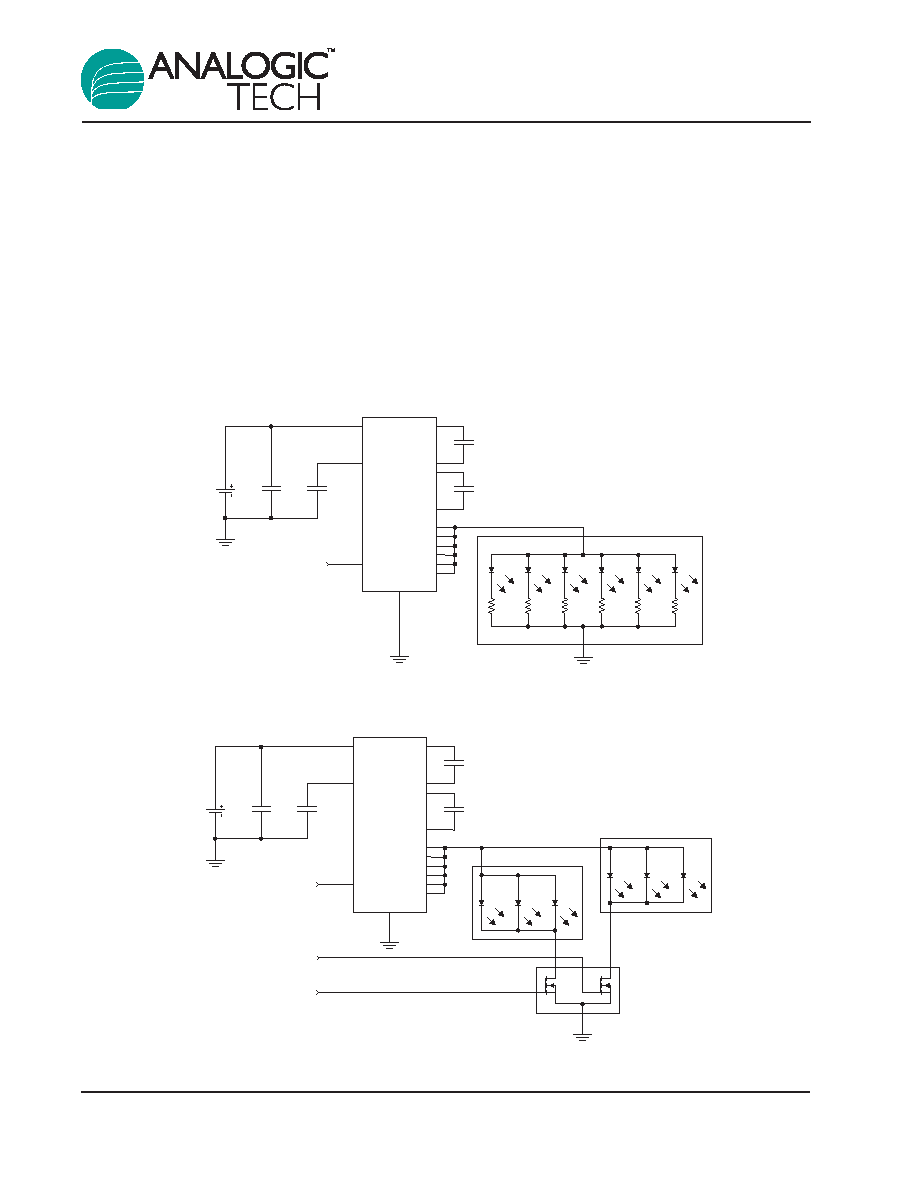
Driving white LED display module backlights
and individual white LEDs connected in parallel:
The AAT3114/14A D1 to D6 outputs are true con-
stant current sources capable of driving up to 20mA
each over the operation input voltage range. Since
these outputs are true constant current sources,
they may be connected in parallel to drive a single
power output. Any combination of outputs (D1 to
D6) may be connected in parallel. The maximum
total output current is a sum of how many current
sources are parallel connected. This feature is par-
ticularly useful to power pre-manufactured display
modules that are pre-wired with white LED back-
lights connected in a parallel circuit configuration. All
outputs can be connected in parallel to drive groups
of LEDs as well. The internal current source refer-
ence circuit bases feedback from current sensed on
the D1 output. For best operation, the only require-
ment for this application is that the output D1 should
always be connected to the load circuit.
AAT3113/13A, AAT3114/14A
High Efficiency 1.5X Fractional Charge
Pumps For White LED Applications
12
3113.2005.11.1.8
AAT3114/14A Application Driving a Display Module With Six Parallel Connected White LEDs:
AAT3114/14A Dual Backlight Control Circuit:
C
IN
1
µ
F
V
BATTERY
C
OUT
1
µ
F
EN/SET
C1
1
µ
F
C2
1
µ
F
D2
D3
D4
V
IN
V
OUT
C1+
C1-
C2+
C2-
D1
D2
D3
D4
EN/SET
GND
AAT3114/14A
D5
D6
D1
D5
D6
Enable Display Backlight
Enable Keyboard Backlight
Display Backlight
Keyboard Backlight
C
IN
1
µ
F
V
BATTERY
C
OUT
1
µ
F
EN/SET
C1
1
µ
F
C2
1
µ
F
D2
D3
D4
D5
V
IN
V
OUT
C1+
C1-
C2+
C2-
D1
D2
D3
D4
EN/SET
GND
AAT3114/14A
D5
D6
D1
D6
Display Module
R
R
R
R
R
R
Resistor R is optional

Ordering Information
Package Information
QFN44-16
All dimensions in millimeters.
4.000
±
0.050
Pin 1 Dot By Marking
2.400
±
0.050
0.600
±
0.050
4.000
±
0.050
2.280 REF
0.650 BSC
0.900
±
0.050
Pin 1 Identification
R0.030Max
1
4
5
8
9
13
16
0.450
±
0.050
0.0125
±
0.0125
0.203
±
0.025
0.330
±
0.050
Top View
Bottom View
Side View
All AnalogicTech products are offered in Pb-free packaging. The term "Pb-free" means
semiconductor products that are in compliance with current RoHS standards, including
the requirement that lead not exceed 0.1% by weight in homogeneous materials. For more
information, please visit our website at http://www.analogictech.com/pbfree.
Package
Marking
1
Part Number (Tape and Reel)
2
TSOPJW-12
HTXYY
AAT3113ITP-20-T1
TSOPJW-12
AAT3113AITP-20-T1
QFN44-16
FGXYY
AAT3114ISN-20-T1
QFN44-16
OVXYY
AAT3114AISN-20-T1
AAT3113/13A, AAT3114/14A
High Efficiency 1.5X Fractional Charge
Pumps For White LED Applications
3113.2005.11.1.8
13
1. XYY = assembly and date code.
2. Sample stock is generally held on all part numbers listed in BOLD.

TSOPJW-12
All dimensions in millimeters.
0.20 + 0.10
- 0.05
0.055
±
0.045
0.45
±
0.15
7
∞
NOM
4
∞ ±
4
∞
3.00
±
0.10
2.40
±
0.10
2.85
±
0.20
0.50 BSC 0.50 BSC 0.50 BSC 0.50 BSC 0.50 BSC
0.15
±
0.05
0.9625
±
0.0375
1.00
+ 0.10
-
0.065
0.04 REF
0.010
2.75
±
0.25
AAT3113/13A, AAT3114/14A
High Efficiency 1.5X Fractional Charge
Pumps For White LED Applications
14
3113.2005.11.1.8
Advanced Analogic Technologies, Inc.
830 E. Arques Avenue, Sunnyvale, CA 94085
Phone (408) 737-4600
Fax (408) 737-4611
© Advanced Analogic Technologies, Inc.
AnalogicTech cannot assume responsibility for use of any circuitry other than circuitry entirely embodied in an AnalogicTech product. No circuit patent licenses, copyrights, mask work rights,
or other intellectual property rights are implied. AnalogicTech reserves the right to make changes to their products or specifications or to discontinue any product or service without notice.
Customers are advised to obtain the latest version of relevant information to verify, before placing orders, that information being relied on is current and complete. All products are sold
subject to the terms and conditions of sale supplied at the time of order acknowledgement, including those pertaining to warranty, patent infringement, and limitation of liability. AnalogicTech
warrants performance of its semiconductor products to the specifications applicable at the time of sale in accordance with AnalogicTech's standard warranty. Testing and other quality con-
trol techniques are utilized to the extent AnalogicTech deems necessary to support this warranty. Specific testing of all parameters of each device is not necessarily performed.