AAT3120
3-Channel Charge Pump
For White LED Applications
3120.2005.11.1.1
1
ChargePump
TM
General Description
The AAT3120 is a low noise, constant frequency
charge pump DC/DC converter that uses fractional
(1.5X) conversion to improve efficiency for white
LED applications. The device can be used to pro-
duce eight current levels up to 20mA per channel
for up to three channels. 1X load switch mode is
also built-in to improve efficiency at low current set-
tings. Low external parts count (two 1µF flying
capacitors and two small 1µF capacitors at V
IN
and
OUT) makes the AAT3120 ideally suited for small
battery-powered applications.
AnalogicTech's S
2
CwireTM (Simple Serial ControlTM)
serial digital input is used to enable, disable, and
set current for each LED at eight different levels.
The AAT3120 has a thermal management system
to protect the device in the event of a short-circuit
condition at the output pin. Built-in soft-start circuit-
ry prevents excessive inrush current during start-
up. A high charge pump switching frequency
enables the use of very small external capacitors.
A low current shutdown feature disconnects the
load from V
IN
and reduces quiescent current to less
than 1µA. The AAT3120 is available in the very
small Pb-free 12-pin TSOPJW package.
Features
∑
V
IN
Range: 2.7V to 5.5V
∑
Fractional Charge Pump Mode
∑
Drives Low-V
F
and High-V
F
Type LEDs
∑
Up to Three LED Outputs
-- Single Wire Programming
-- Eight Regulated Current Settings
-- Max 20mA per Channel
∑
Low Noise Constant Frequency Operation
∑
No Inductors
∑
1MHz Switching Frequency
∑
Small Application Circuit
∑
Automatic Soft-Start
∑
I
Q
<1µA in Shutdown
∑
12-Pin TSOPJW Package
Applications
∑
Color (RGB) Lighting
∑
Programmable Current Source
∑
White LED Backlighting
∑
White Photo Flash for DSCs
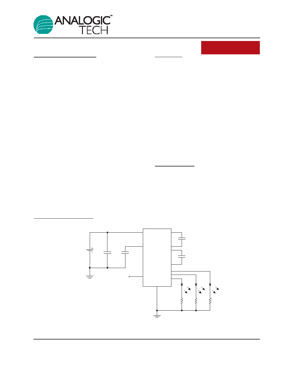
Typical Application
C
IN
1
µF
V
BATTERY
C
OUT
1
µF
EN/SET
C1
1
µF
C2
1
µF
D3
VIN
VOUT
C1+
C1-
C2+
C2-
D1
D2
D3
EN/SET
GND
AAT3120
D2
D1
Pin Descriptions
Pin Configuration
TSOPJW-12
(Top View)
1
2
3
4
5
6
12
11
10
9
8
7
C2+
OUT
C1-
C1+
N/C
D3
C2-
GND
IN
EN/SET
D1
D2
Pin #
Symbol
Function
1
C2+
Flying capacitor 2 positive terminal. Connect a 1µF capacitor between C2+ and
C2-.
2
OUT
Charge pump output. Requires 1µF capacitor connected between this pin and
ground.
3
C1-
Flying capacitor 1 negative terminal.
4
C1+
Flying capacitor 1 positive terminal. Connect a 1µF capacitor between C1+ and
C1-.
5
N/C
No connection.
6
D3
Current source output #3.
7
D2
Current source output #2.
8
D1
Current source output #1.
9
EN/SET
Control pin.
10
IN
Input power supply. Requires 1µF capacitor connected between this pin and
ground.
11
GND
Ground.
12
C2-
Flying capacitor 2 negative terminal.
AAT3120
3-Channel Charge Pump
For White LED Applications
2
3120.2005.11.1.1

Absolute Maximum Ratings
1
T
A
= 25∞C, unless otherwise noted.
Thermal Information
3
Symbol
Description
Value
Units
JA
Thermal Resistance
160
∞C/W
P
D
Maximum Power Dissipation
4
0.625
W
Symbol
Description
Value
Units
V
IN
Input Voltage
-0.3 to 6
V
V
OUT
Charge Pump Output
-0.3 to 6
V
V
EN/SET
FB or EN/SET to GND Voltage
-0.3 to 6
V
V
EN/SET(MAX)
Maximum EN/SET to Input Voltage
0.3
V
I
OUT
2
Maximum DC Output Current
150
mA
T
J
Operating Junction Temperature Range
-40 to 150
∞C
T
LEAD
Maximum Soldering Temperature (at leads, 10 sec)
300
∞C
AAT3120
3-Channel Charge Pump
For White LED Applications
3120.2005.11.1.1
3
1. Stresses above those listed in Absolute Maximum Ratings may cause permanent damage to the device. Functional operation at conditions
other than the operating conditions specified is not implied. Only one Absolute Maximum Rating should be applied at any one time.
2. Based on long-term current density limitation.
3. Mounted on an FR4 board.
4. Derate 6.25mW/∞C above 25∞C.

Electrical Characteristics
1
C
IN
= C
OUT
= C
1
= C
2
= 1.0µF; T
A
= -40∞C to +85∞C, unless otherwise noted. Typical values are T
A
= 25∞C,
V
IN
= 3.5V.
Symbol
Description
Conditions
Min
Typ Max Units
Input Power Supply
V
IN
Operation Range
2.7
5.5
V
I
CC
Operating Current
3.0V
V
IN
5.5V, Active,
1.8
3.0
mA
No Load Current
I
SHDN
Shutdown Current
EN = 0
1.0
µA
I
DX
Output Current
3.0
V
IN
5.5
18
20
22
mA
I
(D-Match)
Current Matching Between
VD1:D3 = 3.6, V
IN
= 3.5V
0.5
%
Any Two Outputs
Charge Pump Section
T
SS
Soft-Start Time
200
µs
F
CLK
Clock Frequency
1000
kHz
EN/SET
V
EN(L)
Enable Threshold Low
2.7V
V
IN
5.5V
0.4
V
V
EN(H)
Enable Threshold High
2.7V
V
IN
5.5V
1.4
V
T
EN/SET LO
EN/SET Low Time
0.3
75
µs
T
EN/SET HI
Minimum EN/SET High Time
50
ns
T
OFF
EN/SET Off Timeout
500
µs
Input Current
EN/SET Input Leakage
-1
1
µA
AAT3120
3-Channel Charge Pump
For White LED Applications
4
3120.2005.11.1.1
1. The AAT3120 is guaranteed to meet performance specifications over the -40∞C to +85∞C operating temperature range and is assured
by design, characterization, and correlation with statistical process controls.
Typical Characteristics
I
DIODE
vs. Input Voltage
(3x8.3mA)
Input Voltage (V)
I
DIODE
(mA)
15
18
21
24
27
30
2.7
2.9
3.1
3.3
3.5
3.7
3.9
4.1
4.3
4.5
4.7
4.9
5.1
V
F
= 3.0V
V
F
= 3.2V
V
F
= 3.4V
I
DIODE
vs. Input Voltage
(3x20mA)
Input Voltage (V)
I
DIODE
(mA)
50
53
56
59
62
65
2.7
2.9
3.1
3.3
3.5
3.7
3.9
4.1
4.3
4.5
4.7
4.9
5.1
V
F
= 3.0V
V
F
= 3.2V
V
F
= 3.4V
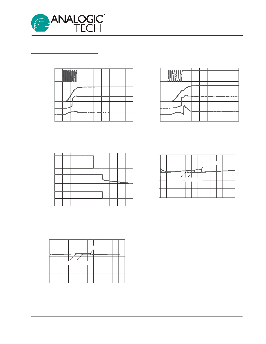
Turn-Off from Full-Scale Charge Pump
Time (400µs/div)
ENSET
(2V/div)
V
DIODE
(2V/div)
I
IN
(100mA/div)
Turn-On to Full-Scale Charge Pump
Time (100µs/div)
ENSET
(2V/div)
CP
(2V/div)
V
DIODE
(2V/div)
I
IN
(200mA/div)
Turn-On to Full-Scale Load Switch
Time (100µs/div)
ENSET
(2V/div)
CP
(2V/div)
V
DIODE
(2V/div)
I
IN
(200mA/div)
AAT3120
3-Channel Charge Pump
For White LED Applications
3120.2005.11.1.1
5

Typical Characteristics
Load Switch to Charge Pump (60mA)
Time (100µs/div)
OUT
(2V/div)
V
DIODE
(2V/div)
V
IN
(10mV/div)
I
IN
(100mA/div)
Charge Pump to Load Switch (60mA)
Time (100µs/div)
OUT
(2V/div)
V
DIODE
(2V/div)
V
IN
(10mV/div)
I
IN
(100mA/div)
60mA Load Characteristics
Time (500ns/div)
OUT
(20mV/div)
V
DIODE
(20mV/div)
V
IN
(20mV/div)
Efficiency vs. Input Voltage
(3x8.3mA)
Input Voltage (V)
Efficiency (%)
50
55
60
65
70
75
80
85
90
95
2.7
2.9
3.1
3.3
3.5
3.7
3.9
4.1
4.3
4.5
4.7
4.9
5.1
V
F
= 3.0V
V
F
= 3.2V
V
F
= 3.4V
Efficiency vs. Input Voltage
(3x20mA)
Input Voltage (V)
Efficiency (%)
50
55
60
65
70
75
80
85
90
95
2.7
2.9
3.1
3.3
3.5
3.7
3.9
4.1
4.3
4.5
4.7
4.9
5.1
V
F
= 3.0V
V
F
= 3.2V
V
F
= 3.4V
AAT3120
3-Channel Charge Pump
For White LED Applications
6
3120.2005.11.1.1

AAT3120
3-Channel Charge Pump
For White LED Applications
3120.2005.11.1.1
7
Functional Block Diagram
1X / 1.5X
Charge
Pump
Soft-Start
Control
1MHz
Oscillator
Voltage
Reference
Quad
Output
DAC
Current
Reference
Single-Wire
Interface
32 x 16 bit
ROM
C1+
C1-
C2+
C2-
OUT
D1
D2
D3
GND
EN/SET
VIN
Functional Description
The AAT3120 is a dual mode load switch (1X) and
high efficiency (1.5X) fractional charge pump
device intended for white LED backlight applica-
tions. The fractional charge pump consists of a low
dropout linear voltage regulator followed by a 1.5X
charge pump with multiple current source outputs.
To maximize power conversion efficiency, an inter-
nal feedback control sensing circuit monitors the
voltage required on the constant current source
outputs. This control circuit then sets the load
switch and charge pump functions based upon the
input voltage level versus the output voltage level
needed. The 1X load switch / 1.5X charge pump
mode is decided on the voltage sensed on the out-
put D1. Switchover between the 1.5X (charge-
pump) operating mode and the 1X (load switch)
mode occurs automatically (as a function of input
and output voltages) and does not require user
intervention to maintain maximum efficiency.
The AAT3120 requires only four external compo-
nents: two 1µF ceramic capacitors for the charge
pump flying capacitors (C1 and C2), one 1µF
ceramic input capacitor (C
IN
), and one 0.33µF to
1µF ceramic output capacitor (C
OUT
). The LDO /
1.5X charge pump output is converted into three
(D1 to D3) constant current outputs to drive three
individual LEDs with a maximum current of 20mA
each. The current source output magnitude is con-
trolled by the EN/SET serial data single-wire inter-
face. The interface records rising edges of the
EN/SET pin and decodes them into eight individual
current level settings (see Table 1, Current Level
Settings). Once the final clock cycle is input for the
desired brightness level, the EN/SET pin is held
high to maintain the device output current at the
programmed level. The device is disabled 500µs
after the EN/SET pin transitions to a logic low state.

AAT3120
3-Channel Charge Pump
For White LED Applications
8
3120.2005.11.1.1
Table 1: Current Level Settings.
Constant Current Output Level Settings
The constant current source output amplitude for
output D1 to D3 is set via the serial interface.
Because the outputs D1 to D3 are true independent
constant current sources, the voltage observed on
any single given output will be determined by the
actual forward voltage (V
F
) for the LED being driven.
Since the output current of the AAT3120 is pro-
grammable through its simple single-wire serial
interface, no PWM (pulse width modulation) or
additional control circuitry is needed to control LED
brightness. This feature greatly reduces the burden
on a microcontroller or system IC to manage LED
or display brightness, allowing the user to "set it
and forget it."
EN/SET Serial Interface
The current source output magnitude is controlled
by the EN/SET serial data single-wire interface.
The interface records rising edges of the EN/SET
pin and decodes them into eight individual current
level settings. Code 8 is full scale.
The counter can be clocked at speeds up to 1MHz,
so intermediate states are not visible. The first rising
edge of EN/SET enables the IC and initially sets the
output LED current to zero. The next lowest setting
is equal to 525µA. Once the final clock cycle is input
for the desired brightness level, the EN/SET pin is
held high to maintain the device output current at
the programmed level. The device is disabled
500µs after the EN/SET pin transitions to a logic low
state. The EN/SET timing is designed to accommo-
date a wide range of data rates. After the first rising
edge of EN/SET, the charge pump is enabled and
reaches full capacity after the soft-start time (T
SS
).
During the soft-start time, multiple clock pulses may
be entered on the EN/SET pin to set the final output
current level with a single burst of clocks.
Alternatively, the EN/SET clock pulses may be
entered one at a time to gradually increase the LED
brightness over any desired time period. A constant
current is sourced as long as EN/SET remains in a
logic high state. The current source outputs are
switched off after EN/SET has remained in a low
state for at least the T
OFF
timeout period.
Test Current/Channel Disable
Each channel of the output is equipped with a test
current function. A small amount of current (~2µA)
is injected into each output current source to detect
the presence of load (LED). For unused channels
that are tied to ground or load LED fail short, those
channels will be automatically disabled instead of
wasting the programmed output current.
Code
I
OUT
, Each LED (mA)
1
0
2
0.5
3
1.3
4
3.3
5
8.3
6
11.1
7
15
8
20
EN/SET Timing
EN/SET
Code
1
2
3
OFF
OFF
t
HI
t
LO
t
OFF

Applications Information
LED Selection
The AAT3120 is specifically intended for driving
white LEDs. However, the device design will allow
the AAT3120 to drive most types of LEDs with for-
ward voltage specifications ranging from 2.0V to
4.3V. LED applications may include main and sub-
LCD display backlighting, camera photo-flash appli-
cations, color (RGB) LEDs, infrared (IR) diodes for
remotes, and other loads benefiting from a controlled
output current generated from a varying input volt-
age. Since the D1 to D3 output current sources are
matched with negligible voltage dependence, the
LED brightness will be matched regardless of the
specific LED forward voltage (V
F
) levels.
In some instances (e.g., in high-luminous-output
applications such as photo-flash) it may be neces-
sary to drive high-V
F
type LEDs. The low-dropout
current-sources in the AAT3120 make it capable of
driving LEDs with forward voltages as high as 4.3V
at full current from an input supply as low as 3.0V.
Outputs can be paralleled to drive high current
LEDs without complication.
Device Switching Noise Performance
The AAT3120 operates at a fixed frequency of
approximately 1MHz to control noise and limit har-
monics that can interfere with the RF operation of
cellular telephone handsets or other communica-
tion devices. Back-injected noise appearing on the
input pin of the charge pump is 20mV peak-to-
peak, typically ten times less than inductor-based
DC/DC boost converter white LED backlight solu-
tions. The AAT3120 soft-start feature prevents
noise transient effects associated with in-rush cur-
rents during start up of the charge pump circuit.
Power Efficiency and Device
Evaluation
The charge pump efficiency discussion in the fol-
lowing sections only accounts for efficiency of the
charge pump section itself. Due to the unique circuit
architecture and design of the AAT3120, it is very
difficult to measure efficiency in terms of a percent
value comparing input power over output power.
Since the AAT3120 outputs are pure constant cur-
rent sources and typically drive individual loads, it is
difficult to measure the output voltage for a given
output (D1 to D3) to derive an overall output power
measurement. For any given application, white LED
forward voltage levels can differ, yet the output drive
current will be maintained as a constant. This makes
quantifying output power a difficult task when taken
in the context of comparing to other white LED driv-
er circuit topologies. A better way to quantify total
device efficiency is to observe the total input power
to the device for a given LED current drive level. The
best white LED driver for a given application should
be based on trade-offs of size, external components
count, reliability, operating range, and total energy
usage...not just % efficiency.
The AAT3120 efficiency may be quantified under
very specific conditions and is dependent upon the
input voltage versus the output voltage seen
across the loads applied to outputs D1 through D3
for a given constant current setting. Depending
upon the case of V
IN
being greater than the specif-
ic voltage seen across the load on D1, the device
will operate in "load switch" mode. If the voltage
seen on the constant current source output is less
than V
IN
, then the device will operate in 1.5X
charge pump mode. Each of these two modes will
yield different efficiency values. One should refer
to the following two sections for explanations of
each operational mode.
Load Switch Mode Efficiency
The AAT3120 load switch mode is operational at all
times. It functions alone to enhance device power
conversion efficiency when the condition exists
where V
IN
is greater than the voltages at the con-
stant current source outputs. When in "load switch"
mode, the voltage conversion efficiency is defined
as output power divided by input power:
=
P
OUT
P
IN
AAT3120
3-Channel Charge Pump
For White LED Applications
3120.2005.11.1.1
9

AAT3120
3-Channel Charge Pump
For White LED Applications
10
3120.2005.11.1.1
The expression to define the ideal efficiency (
)
can be rewritten as:
-or-
Charge Pump Section Efficiency
The AAT3120 contains a fractional charge pump
which will boost the input supply voltage in the
event where V
IN
is less than the voltage required
on the constant current source outputs. The effi-
ciency (
) can be simply defined as a linear voltage
regulator with an effective output voltage that is
equal to one and one half times the input voltage.
Efficiency (
) for an ideal 1.5X charge pump can
typically be expressed as the output power divided
by the input power.
In addition, with an ideal 1.5X charge pump, the
output current may be expressed as 2/3 of the
input current. The expression to define the ideal
efficiency (
) can be rewritten as:
-or-
For a charge pump with an output of 5 volts and a
nominal input of 3.5 volts, the theoretical efficiency
is 95%. Due to internal switching losses and IC
quiescent current consumption, the actual efficien-
cy can be measured at 93%. These figures are in
close agreement for output load conditions from
1mA to 100mA. Efficiency will decrease as load
current drops below 0.05mA or when level of V
IN
approaches V
OUT
. Refer to the Typical Character-
istics section of this document for measured plots
of efficiency versus input voltage and output load
current for the given charge pump output voltage
options.
Ballast Resistors for Current Matching
In some applications, white LED forward voltages
can vary significantly. Ballast resistors between
the LED cathodes and ground are recommended
for balancing the forward voltage differences. The
ballast resistor value may be approximated by the
following equation:
Capacitor Selection
Careful selection of the four external capacitors
C
IN
, C
1
, C
2
, and C
OUT
is important because they will
affect turn-on time, output ripple, and transient per-
formance. Optimum performance will be obtained
when low Equivalent Series Resistance (ESR)
ceramic capacitors are used. In general, low ESR
may be defined as less than 100m
. A value of
1µF for all four capacitors is a good starting point
when choosing capacitors. If the LED current
sources are only programmed for light current lev-
els, then the capacitor size may be decreased.
Capacitor Characteristics
Ceramic composition capacitors are highly recom-
mended over all other types of capacitors for use with
the AAT3120. Ceramic capacitors offer many advan-
tages over their tantalum and aluminum electrolytic
counterparts. A ceramic capacitor typically has very
low ESR, is lowest cost, has a smaller PCB footprint,
and is non-polarized. Low ESR ceramic capacitors
help maximize charge pump transient response.
Since ceramic capacitors are non-polarized, they are
not prone to incorrect connection damage.
Equivalent Series Resistance
R
B
=
V
SOURCE
- V
F
I
F
(%) = 100
V
OUT
1.5V
IN
=
P
OUT
=
V
OUT
◊ I
OUT
=
V
OUT
P
IN
V
IN
◊ 1.5I
OUT
1.5V
IN
=
P
OUT
P
IN
(%) = 100
V
OUT
V
IN
=
P
OUT
=
V
OUT
◊ I
OUT
=
V
OUT
P
IN
V
IN
◊ I
OUT
V
IN

AAT3120
3-Channel Charge Pump
For White LED Applications
3120.2005.11.1.1
11
ESR is an important characteristic to consider when
selecting a capacitor. ESR is a resistance internal
to a capacitor, which is caused by the leads, inter-
nal connections, size or area, material composition,
and ambient temperature. Capacitor ESR is typi-
cally measured in milliohms for ceramic capacitors
and can range to more than several ohms for tan-
talum or aluminum electrolytic capacitors.
Ceramic Capacitor Materials
Ceramic capacitors less than 0.1µF are typically
made from NPO or C0G materials. NPO and C0G
materials typically have tight tolerance and are sta-
ble over temperature. Large capacitor values are
typically composed of X7R, X5R, Z5U, or Y5V
dielectric materials. Large ceramic capacitors, typ-
ically greater than 2.2µF, are often available in low-
cost Y5V and Z5U dielectrics, but capacitors
greater than 1µF are typically not required for
AAT3120 applications.
Capacitor area is another contributor to ESR.
Capacitors that are physically large will have a lower
ESR when compared to an equivalent material
smaller capacitor. These larger devices can improve
circuit transient response when compared to an
equal value capacitor in a smaller package size.
Thermal Protection
The AAT3120 has a thermal protection circuit that
will shut down the internal LDO and charge pump
if the die temperature rises above the thermal limit,
as is the case during a short circuit of the OUT pin.
Charge Pump Compatibility
The AAT3120 is pin-compatible with the AAT3113
in TSOPJW-12 packages, with no D4 output.
Compared to the AAT3113, the AAT3120 offers an
improved overall efficiency, wider operating range,
and the ability to drive high-V
F
type LEDs (up to
4.3V) at full current from a 3V input condition. The
AAT3120 is well suited for battery-powered appli-
cations using single-cell Lithium-Ion (Li-Ion) batter-
ies (4.2V to 2.8V), Lithium Polymer batteries, and
3-series connected dry cells (3.6V).

AAT3120
3-Channel Charge Pump
For White LED Applications
12
3120.2005.11.1.1
Additional Application Circuits
AAT3120 Driving a Display Module with Three Paralleled White LEDs.
AAT3120 Driving Common-Anode RGB Color LED.
C
IN
1
µF
V
BATTERY
C
OUT
1
µF
EN/SET
C1
1
µF
C2
1
µF
RED
VIN
VOUT
C1+
C1-
C2+
C2-
D1
D2
D3
EN/SET
GND
AAT3120
GRN
Enable Green
Enable Red
Enable Blue
BLU
Common-Anode
RGB Color LED
R
R
R
C
IN
1
µF
V
BATTERY
C
OUT
1
µF
EN/SET
C1
1
µF
C2
1
µF
D2
D3
VIN
VOUT
C1+
C1-
C2+
C2-
D1
D2
D3
EN/SET
GND
AAT3120
D1
Display Module
R
R
R

Ordering Information
Package Information
All dimensions in millimeters.
0.20 + 0.10
- 0.05
0.055
±
0.045
0.45
±
0.15
7
∞
NOM
4
∞ ±
4
∞
3.00
±
0.10
2.40
±
0.10
2.85
±
0.20
0.50 BSC 0.50 BSC 0.50 BSC 0.50 BSC 0.50 BSC
0.15
±
0.05
0.9625
±
0.0375
1.00
+ 0.10
-
0.065
0.04 REF
0.010
2.75
±
0.25
All AnalogicTech products are offered in Pb-free packaging. The term "Pb-free" means
semiconductor products that are in compliance with current RoHS standards, including
the requirement that lead not exceed 0.1% by weight in homogeneous materials. For more
information, please visit our website at http://www.analogictech.com/pbfree.
Package
Marking
1
Part Number (Tape and Reel)
2
TSOPJW-12
NGXYY
AAT3120ITP-T1
AAT3120
3-Channel Charge Pump
For White LED Applications
3120.2005.11.1.1
13
1. XYY = assembly and date code.
2. Sample stock is generally held on part numbers listed in BOLD.

AAT3120
3-Channel Charge Pump
For White LED Applications
14
3120.2005.11.1.1
Advanced Analogic Technologies, Inc.
830 E. Arques Avenue, Sunnyvale, CA 94085
Phone (408) 737-4600
Fax (408) 737-4611
© Advanced Analogic Technologies, Inc.
AnalogicTech cannot assume responsibility for use of any circuitry other than circuitry entirely embodied in an AnalogicTech product. No circuit patent licenses, copyrights, mask work rights,
or other intellectual property rights are implied. AnalogicTech reserves the right to make changes to their products or specifications or to discontinue any product or service without notice.
Customers are advised to obtain the latest version of relevant information to verify, before placing orders, that information being relied on is current and complete. All products are sold
subject to the terms and conditions of sale supplied at the time of order acknowledgement, including those pertaining to warranty, patent infringement, and limitation of liability. AnalogicTech
warrants performance of its semiconductor products to the specifications applicable at the time of sale in accordance with AnalogicTech's standard warranty. Testing and other quality con-
trol techniques are utilized to the extent AnalogicTech deems necessary to support this warranty. Specific testing of all parameters of each device is not necessarily performed.