AAT3131
High Efficiency 1X/1.5X Fractional
Charge Pump for White LED Applications
3131.2004.05.1.0
1
ChargePump
TM
General Description
The AAT3131 is a low noise, constant frequency
charge pump DC/DC converter that uses a dual
mode Load Switch (1X) and fractional (1.5X) con-
version to maximize efficiency for White LED appli-
cations. The device can be used to produce cur-
rent levels up to 20mA in three of its outputs, and
30mA in one of its outputs to drive LEDs from a
2.7V to 5.5V input. Outputs may be operated indi-
vidually or paralleled for driving higher-current
LEDs. Low external parts counts (two 1µF flying
capacitors and two small 1µF capacitors at V
IN
,
and OUT) make the AAT3131 ideally suited for
small battery-powered applications.
AnalogicTechTM's Simple Serial ControlTM
(S
2
CwireTM) interface is used to enable, disable
and set the LED drive current in two groups: the
three 20mA outputs and the single 30mA output
with multiple level logarithmic scales. The AAT3131
has a thermal management system to protect the
device in the event of a short circuit condition at the
output pin. Built-in soft-start circuitry prevents
excessive inrush current during start-up. A high
charge pump switching frequency enables the use
of very small external capacitors. A low current
shutdown feature disconnects the load from V
IN
and reduces quiescent current to less than 1µA.
The AAT3131 is available in very small 12 pin
TSOPJW12 package.
Features
∑
V
IN
Range: 2.7 - 5.5 Volts
∑
< 1.0µA of Shutdown current
∑
1.0 MHz Switching Frequency
∑
White LED Backlighting
∑
Fully Independent Display Lighting
∑
Dual Mode 1x and 1.5x Charge Pump for
Maximum Efficiency
∑
Drives Low-V
F
& High-V
F
f Type LED's
∑
Up to three 20mA Outputs
∑
Single 30 mA Output
∑
Multi Position Logarithmic Scale with Digital
Control
∑
Low Noise Constant Frequency Operation
∑
Regulated Output Current
∑
Automatic Soft-Start
∑
No Inductors
∑
-40 to +85∞C Temperature Range
∑
12 pin TSOPJW-12 package
Applications
∑
White LED Backlighting
∑
White Photo-Flash for DSC's
∑
Color (RGB) Lighting
∑
Programmable Current Source
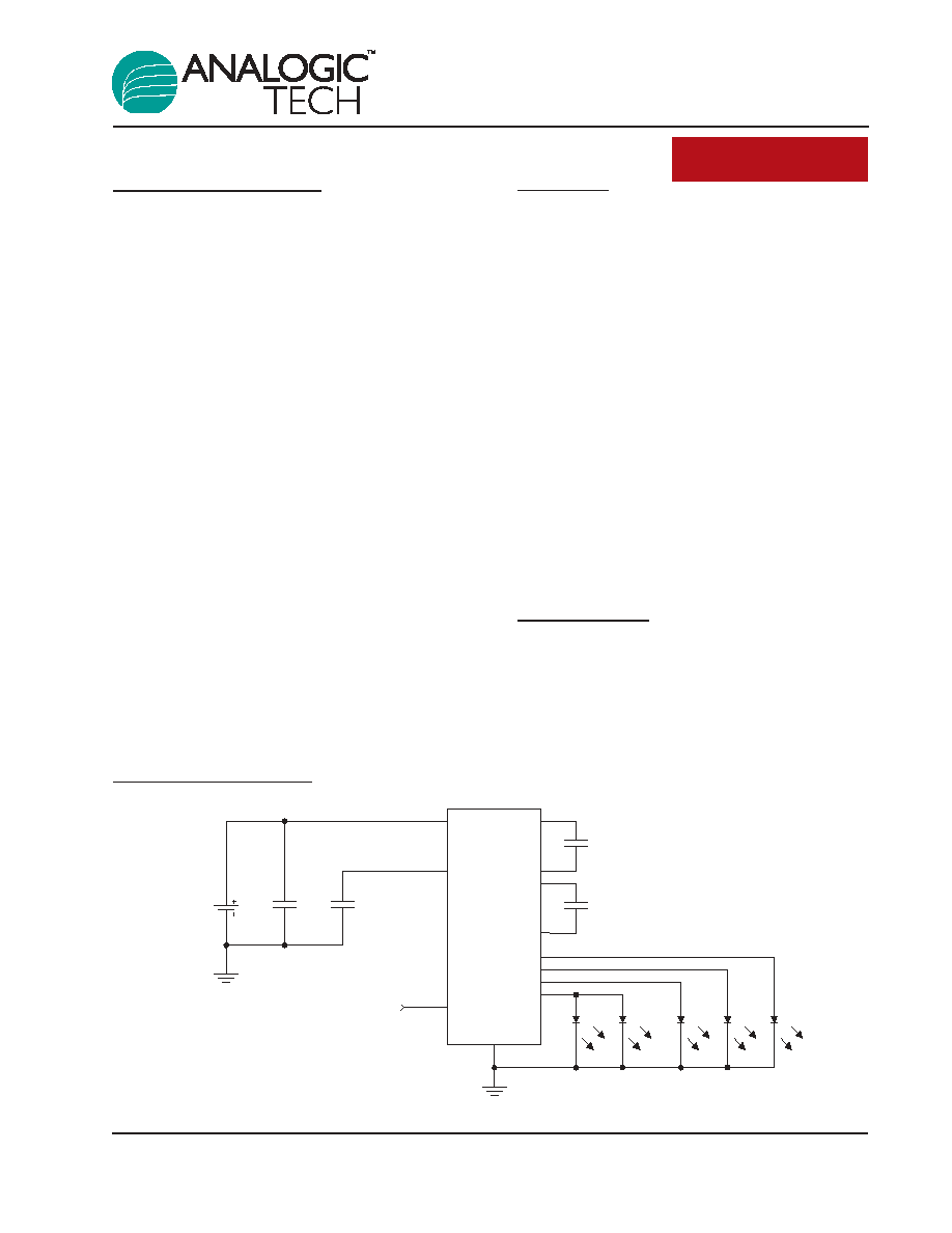
Typical Application
C
IN
1
µF
V
BATTERY
C
OUT
1
µF
EN/SET
C1
1
µF
C2
1
µF
D5
D3
D2
D1
V
IN
V
OUT
C1+
C1-
C2+
C2-
D1
D2
D3
D4
EN/SET
GND
AAT3131
D4
Pin Descriptions
Pin Configuration
TSOPJW-12
(Top view)
1
2
3
4
5
6
12
11
10
9
8
7
C2+
OUT
C1-
C1+
D3
D2
C2-
GND
IN
EN/SET
D1
D4
Pin #
Symbol
Function
1
C2+
Flying Capacitor 2 + terminal. Connect a 1µF capacitor between C2+ and C2-.
2
OUT
Charge pump output. Requires 1µF capacitor connected between this pin and
ground.
3
C1-
Flying Capacitor 1 - terminal
4
C1+
Flying Capacitor 1 + terminal. Connect a 1µF capacitor between C1+ and C1-.
5
D3
Current source output #4
6
D2
Current source output #3
7
D4
Current source output #2
8
D1
Current source output #1
9
EN/SET
Control Pin
10
IN
Input power supply. Requires 1µF capacitor connected between this pin and
ground.
11
GND
Ground
12
C2-
Flying Capacitor 2 - terminal
AAT3131
High Efficiency 1X/1.5X Fractional
Charge Pump for White LED Applications
2
3131.2004.05.1.0

Absolute Maximum Ratings
1
Notes:
1. Stresses above those listed in Absolute Maximum Ratings may cause permanent damage to the device. Functional operation at condi-
tions other than the operating conditions specified is not implied. Only one Absolute Maximum rating should be applied at any one time.
2. Based on long-term current density limitation.
Thermal Information
Notes:
1. Mounted on a FR4 board.
2. Derate 6.25mW/∞C above 25∞C.
Symbol
Description
Value
Units
JA
Thermal Resistance
1
160
∞C/W
P
D
Maximum Power Dissipation
1, 2
(T
A
= 25∞C)
625
mW
Symbol
Description
Value
Units
V
IN
Input Voltage
-0.3 to 6
V
V
OUT
Charge Pump Output
-0.3 to 6
V
F
B
, V
EN/SET
FB or EN/SET to GND Voltage
-0.3 to 6
V
V
EN/SET(MAX)
Maximum EN/SET to Input Voltage
V
IN
- 0.3
V
I
OUT
(2)
Maximum DC Output Current
150
mA
T
J
Operating Junction Temperature Range
-40 to 150
∞C
T
LEAD
Maximum Soldering Temperature (at leads, 10 sec)
300
∞C
AAT3131
High Efficiency 1X/1.5X Fractional
Charge Pump for White LED Applications
3131.2004.05.1.0
3

Electrical Characteristics
1
V
IN
= 3.5V, C
IN
= C
OUT
= C1 = C2 = 1.0µF; T
A
= -40 to 85∞C unless otherwise noted. Typical values are T
A
= 25∞C.
Notes:
1. The AAT3131 is guaranteed to meet performance specification over the -40 to 85∞C operating temperature range and are assured by
design, characterization and correlation with statistical process controls.
Symbol
Description
Conditions
Min
Typ
Max
Units
Input Power Supply
V
IN
Operation Range
2.7
5.5
V
I
CC
Operating Current
3.0
V
IN
5.5, Active,
1.8
3.5
mA
No Load Current
I
SHDN
Shutdown Current
EN = 0
1.0
µA
I
DX
Max. Output Current D1 to D3
3.0
V
IN
5.5
18
20
22
mA
I
DX
Max. Output Current D4
3.0
V
IN
5.5
27
30
33
mA
I
(D-Match)
Current Matching between
VD1:D3 = 3.6, V
IN
= 3.3V
0.5
%
any two outputs
CP
Charge Pump Section Efficiency
V
IN
= 3.5V, I
OUT(TOTAL)
= 90mA,
93
%
Measured from IN to OUT
Charge Pump Section
T
SS
Soft start time
200
µs
F
CLK
Clock Frequency
1000
kHz
EN/SET
V
EN(L)
Enable Threshold Low
0.5
V
V
EN(H)
Enable Threshold High
1.4
V
T
EN/SET LO
EN/SET low time
V
EN/SET
< 0.5
0.3
75
µs
T
EN/SET HI
Minimum EN/SET high time
V
EN/SET
> 1.4
50
ns
T
OFF
EN/SET Off Timeout
V
EN/SET
< 0.5
500
µs
Input Current EN/SET input leakage
-1
1
µA
AAT3131
High Efficiency 1X/1.5X Fractional
Charge Pump for White LED Applications
4
3131.2004.05.1.0
AAT3131
High Efficiency 1X/1.5X Fractional
Charge Pump for White LED Applications
3131.2004.05.1.0
5
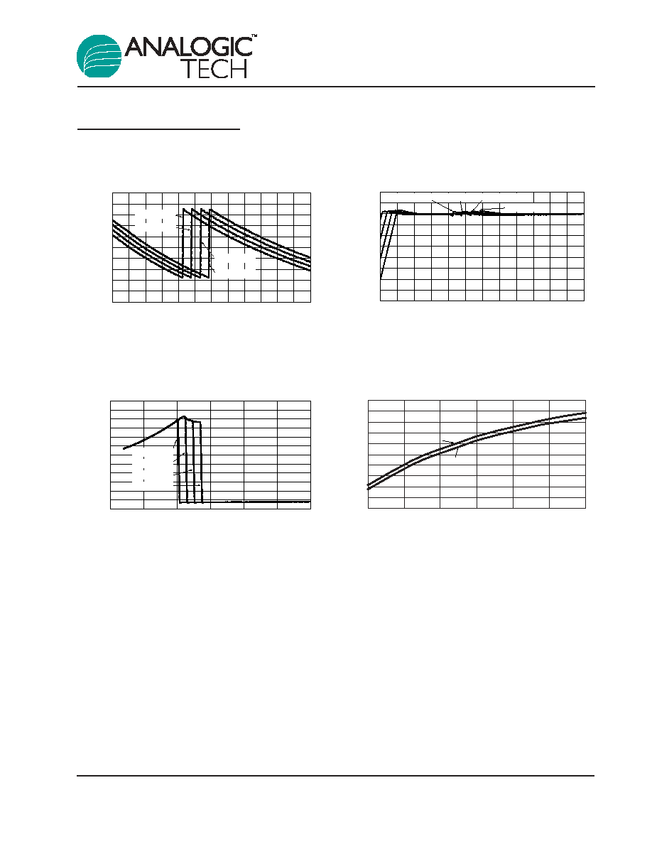
Typical Characteristics
(Unless otherwise noted, V
IN
= 3.5V, C
IN
= C
OUT
= C1 = C2 = 1µF, T
A
= 25∞C)
V
IH
and V
IL
vs. V
IN
0.600
0.625
0.650
0.675
0.700
0.725
0.750
0.775
0.800
0.825
0.850
2.5
3.0
3.5
4.0
4.5
5.0
5.5
V
IN
(V)
V
IH
V
IL
Quiescent Current vs. V
IN
0.0
0.2
0.4
0.6
0.8
1.0
1.2
1.4
1.6
1.8
2.0
2.2
2.4
2.50
3.00
3.50
4.00
4.50
5.00
5.50
V
IN
(V)
Quiescent Current (mA)
V
DIODE
= 3.3V
V
DIODE
= 3.4V
V
DIODE
= 3.5V
V
DIODE
= 3.6V
I
DIODE
vs. V
IN
(4x20mA)
40
45
50
55
60
65
70
75
80
85
90
2.7 2.9
3.1 3.3
3.5
3.7
3.9
4.1 4.3
4.5
4.7 4.9
5.1
V
IN
(V)
I
DIODE
(mA)
V
DIODE
= 3.3V
V
DIODE
= 3.4V V
DIODE
= 3.5V
V
DIODE
= 3.6V
Efficiency vs. VIN (4x20mA)
50%
55%
60%
65%
70%
75%
80%
85%
90%
95%
100%
2.7 2.9
3.1 3.3
3.5 3.7 3.9
4.1 4.3
4.5
4.7 4.9
5.1
V
IN
(V)
Efficiency
V
DIODE
= 3.3V
V
DIODE
= 3.4V
V
DIODE
= 3.5V
V
DIODE
= 3.6V