
SmartSwitch
TM
AAT4601A
1.8A Current Limited P-Channel Switch
4601A.2006.03.1.4
1
General Description
The AAT4601A SmartSwitch is a member of
AnalogicTech's Application Specific Power
MOSFETTM (ASPMTM) product family. It is a 1.8A
current limited P-channel MOSFET power switch
designed for high-side load switching applications.
This switch operates with inputs ranging from 2.7V
to 5.5V, making it ideal for both 3V and 5V systems.
An integrated current-limiting circuit protects the
input supply against large changes in load current
which could cause the supply to fall out of regula-
tion. The AAT4601A has protection from thermal
overload which limits power dissipation and junction
temperatures. The maximum current limit level will
guarantee that 1.8A can be delivered to the load;
the actual threshold is programmed with a resistor
from the SET pin to ground. The quiescent supply
current is typically 12µA. In shutdown mode, the
supply current decreases to less than 1µA.
The AAT4601A is available in a Pb-free, 8-pin SOP,
TSSOP, or MSOP package and is specified over
the -40∞C to +85∞C temperature range.
Features
∑
Input Voltage: 2.7V to 5.5V
∑
Programmable Over-Current Threshold
∑
Low Quiescent Current
-- 12µA Typical
-- Less Than 1µA with Switch Off
∑
Only 2.5V Needed for ON Control
∑
Thermal Shutdown
∑
Fault Flag
∑
2ms Fault Blanking
∑
Under-Voltage Lockout
∑
Temperature Range: -40∞C to +85∞C
∑
4kV ESD rating
∑
UL Approved--File No. E217765
∑
8-Pin SOP, TSSOP, or MSOP Package
Applications
∑
Hot Swap Supplies
∑
Notebook Computers
∑
Peripheral Ports
∑
USB Ports
UL Recognized Component
Typical Application
AAT4601A
ON
IN
OUT
SET
GND
ON
1µF
100k
R
SET
1µF
INPUT
OUTPUT
IN
OUT
FAULT
1
2
8
3
6
7
5
4

Pin Descriptions
Pin Configuration
SOP-8
MSOP-8
(Top View)
(Top View)
TSSOP-8
(Top View)
IN
IN
ON
GND
FAULT
OUT
OUT
SET
4
3
2
1
5
6
7
8
1
2
OUT
FAULT
OUT
SET
IN
IN
ON
GND
1
2
3
4
8
7
6
5
1
2
OUT
FAULT
OUT
SET
IN
IN
ON
GND
1
2
3
4
8
7
6
5
Pin #
Symbol
Function
1, 2
IN
These pins are the input to the P-channel MOSFET source. Connect a
1µF capacitor from IN to GND.
3
ON
Active low enable input. A logic low turns the switch on.
4
GND
Ground.
5
SET
Current limit set input. A resistor from SET to ground sets the current limit
for the switch.
6, 7
OUT
These pins are the P-channel MOSFET drain connection. Connect a 1µF
capacitor from OUT to GND.
8
FAULT
Fault indication output. This open-drain output goes low when in current
limit or when the die temperature exceeds +135∫C, with a 2ms delay after
the fault event occurs.
AAT4601A
1.8A Current Limited P-Channel Switch
2
4601A.2006.03.1.4
AAT4601A
1.8A Current Limited P-Channel Switch
4601A.2006.03.1.4
3
Absolute Maximum Ratings
1
T
A
= 25∞C, unless otherwise noted.
Thermal Characteristics
3
Symbol
Description
Value
Units
SOP-8
100
JA
Maximum Thermal Resistance
TSSOP-8
150
∞C/W
MSOP-8
150
SOP-8
1.25
W
P
D
Maximum Power Dissipation
TSSOP-8
833
mW
MSOP-8
833
Symbol
Description
Value
Units
V
IN
IN to GND
-0.3 to 6
V
V
ON,
V
FAULT
ON, FAULT to GND
-0.3 to V
IN
+ 0.3
V
V
SET,
V
OUT
SET, OUT to GND
-0.3 to V
IN
+ 0.3
V
I
MAX
Maximum Continuous Switch Current
3
A
T
J
Operating Junction Temperature Range
-40 to 150
∞C
T
LEAD
Maximum Soldering Temperature (at Leads)
300
∞C
V
ESD
ESD Rating--HBM
2
4000
V
1. Stresses above those listed in Absolute Maximum Ratings may cause permanent damage to the device. Functional operation at condi-
tions other than the operating conditions specified is not implied. Only one Absolute Maximum Rating should be applied at any one time.
2. Human body model is a 100pF capacitor discharged through a 1.5k
resistor into each pin.
3. Mounted on an FR4 printed circuit board.
AAT4601A
1.8A Current Limited P-Channel Switch
4
4601A.2006.03.1.4
Electrical Characteristics
V
IN
= 5V, T
A
= -40∞C to +85∞C, unless otherwise noted. Typical values are T
A
= 25∞C.
Symbol
Description
Conditions
Min
Typ
Max
Units
V
IN
Operation Voltage
2.7
5.5
V
I
Q
Quiescent Current
V
IN
= 5V, ON = GND, I
OUT
= 0
12
30
µA
I
Q(OFF)
Off-Supply Current
ON = IN, V
IN
= 5.5V
0.004
1
µA
I
SD(OFF)
Off-Switch Current
ON = IN, V
IN
= 5.5V, V
OUT
= 0
0.07
15
µA
V
UVLO
Under-Voltage Lockout
Rising Edge, 1% Hysteresis
2.0
2.3
2.7
V
V
IN
= 5.0V
70
R
DS(ON)
On Resistance
V
IN
= 4.5V
75
130
V
IN
= 3.0V
80
150
m
V
IN
= 3.0V, T
A
= 25∞C
80
110
I
LIM
Current Limit
R
SET
= 20.5k
750
1000
1250
mA
I
LIM(MIN)
Minimum Current Limit
260
mA
OTMP
Shutdown Temperature
V
IN
= 5V
125
∫C
V
ONL
ON Input Low Voltage
0.8
V
V
ONH
ON Input High Voltage
V
IN
= 2.7V to 3.6V
2.0
V
IN
= 4.5V to 5.5V
2.4
V
I
ONSINK
ON Input leakage
V
ON
= 5.5V
0.01
1
µA
V
FAULTL
FAULT Logic Output Low Voltage
I
SINK
= 1mA
0.08
0.4
V
I
FSINK
FAULT Logic Output High Leakage
V
FAULT
= 5.5V
0.05
1
µA
T
RESP
Current Limit Response Time
V
IN
= 5V
2
µs
T
BLANK
Fault Blanking Time After Turn-On
2
ms
T
OFF
Turn-Off Time
1
V
IN
= 5V
20
µs
T
ON
Turn-On Time
1
V
IN
= 5V
200
µs
1. Guaranteed by design.
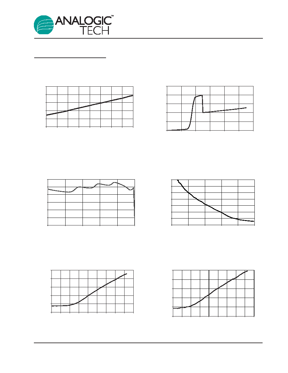
Typical Characteristics
Unless otherwise noted, V
IN
= 5V, T
A
= 25∞C.
Off-Switch Current vs. Temperature
1
0.1
0.01
0.001
0.0001
10
-40
-20
0
20
40
60
80
100
120
140
Temperature (
∞
C)
Off-Switch Current (
µ
A)
Off-Supply Current vs. Temperature
0.0001
0.001
0.01
0.1
1
10
-40
-20
0
20
40
60
80
100
120
140
Temperature
Off-Supply Current (
µ
A)
(
∞
C)
R
SET
* I
LIM
Product vs. I
LIM
Typical I
LIM
(A)
Product (V)
18000
19000
20000
21000
22000
23000
24000
25000
0.0
0.5
1.0
1.5
2.0
2.5
Current Limit
(R
SET
= 20.5k
; V
IN
= 5.0V)
Output Voltage (V)
Output Current (A)
0.0
0.2
0.4
0.6
0.8
1.0
1.2
0
1
2
3
4
5
0
0
1
2
3
4
5
6
5
10
15
20
25
Quiescent Current
Input Voltage (V)
Input Curent (
µ
A)
Quiescent Current vs. Temperature
0
5
10
15
20
25
-40
-20
0
20
40
60
80
100
120
Temperature (
∞
C)
Quiescent Current (
µ
A)
AAT4601A
1.8A Current Limited P-Channel Switch
4601A.2006.03.1.4
5