 | –≠–Ľ–Ķ–ļ—ā—Ä–ĺ–Ĺ–Ĺ—č–Ļ –ļ–ĺ–ľ–Ņ–ĺ–Ĺ–Ķ–Ĺ—ā: AAT8543 | –°–ļ–į—á–į—ā—Ć:  PDF PDF  ZIP ZIP |

General Description
The AAT8543 is a low threshold P-channel MOSFET
designed for the battery, cell phone, and PDA mar-
kets. Using AnalogicTech's ultra-high-density MOS-
FET process and space-saving, small-outline, J-lead
package, performance superior to that normally
found in a TSOP-6 footprint has been squeezed into
the footprint of an SC70JW-8 package.
Applications
∑
Battery Packs
∑
Battery-Powered Portable Equipment
∑
Cellular and Cordless Telephones
Features
∑
Drain-Source Voltage (max): -20V
∑
Continuous Drain Current
1
(max):
-4.2A @ 25įC
∑
Low On-Resistance:
-- 57m
@ V
GS
= -4.5V
-- 104m
@ V
GS
= -2.5V
SC70JW-8 Package
D
D
D
D
S
S
S
G
Top View
1
2
3
4
8
7
6
5
AAT8543
20V P-Channel Power MOSFET
Absolute Maximum Ratings
T
A
= 25įC, unless otherwise noted.
Thermal Characteristics
1
Symbol
Description
Typ
Max
Units
R
JA
Typical Junction-to-Ambient Steady State
100
124
įC/W
R
JA2
Maximum Junction-to-Ambient t<5 Seconds
62
76
įC/W
R
JF
Typical Junction-to-Foot
35
42
įC/W
P
D
Maximum Power Dissipation
T
A
= 25įC
1.6
W
T
A
= 70įC
1.0
Symbol
Description
Value
Units
V
DS
Drain-Source Voltage
-20
V
V
GS
Gate-Source Voltage
Ī12
I
D
Continuous Drain Current @ T
J
= 150įC
1
T
A
= 25įC
Ī4.2
T
A
= 70įC
Ī3.3
A
I
DM
Pulsed Drain Current
2
Ī20
I
S
Continuous Source Current (Source-Drain Diode)
1
-1.2
T
J
Operating Junction Temperature Range
-55 to 150
įC
T
STG
Storage Temperature Range
-55 to 150
įC
8543.2005.04.1.0
1
1. Based on thermal dissipation from junction to ambient while mounted on a 1" x 1" PCB with optimized layout. A 5-second pulse on a
1" x 1" PCB approximates testing a device mounted on a large multi-layer PCB as in most applications. R
JF
+ R
FA
= R
JA
where the
foot thermal reference is defined as the normal solder mounting surface of the device's leads. R
JF
is guaranteed by design; howev-
er, R
CA
is determined by the PCB design. Actual maximum continuous current is limited by the application's design.
2. Pulse test: Pulse Width = 300Ķs.
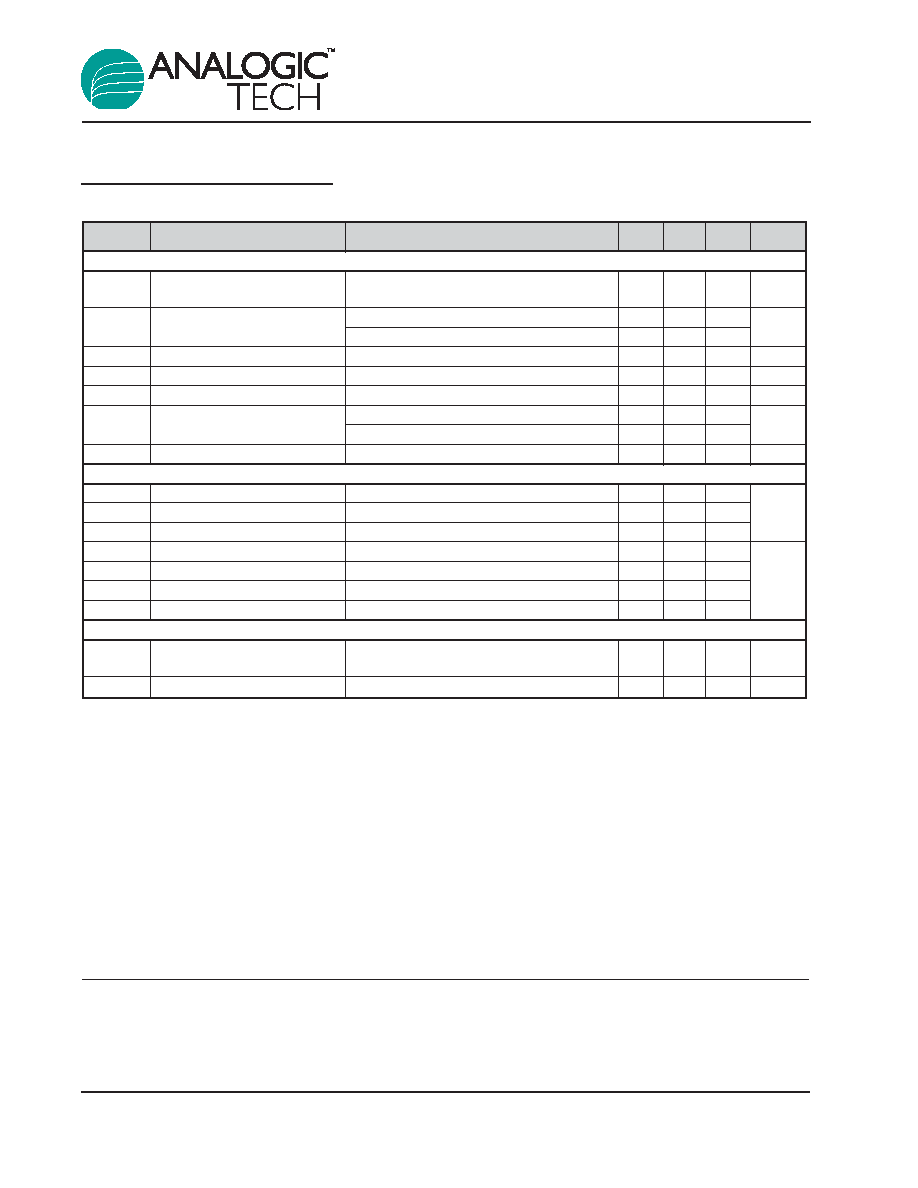
Electrical Characteristics
T
J
= 25įC, unless otherwise noted.
Symbol Description
Conditions
Min
Typ Max
Units
DC Characteristics
BV
DSS
Drain-Source Breakdown
V
GS
= 0V, I
D
= -250ĶA
-20
V
Voltage
R
DS(ON)
Drain-Source On-Resistance
1
V
GS
= -4.5V, I
D
= -4.2A
45
57
m
V
GS
= -2.5V, I
D
= -3.1A
80
104
I
D(ON)
On-State Drain Current
1
V
GS
= -4.5V, V
DS
= -5V (pulsed)
-20
A
V
GS(th)
Gate Threshold Voltage
V
GS
= V
DS
, I
D
= -250ĶA
-0.6
V
I
GSS
Gate-Body Leakage Current
V
GS
= Ī12V, V
DS
= 0V
Ī100
nA
I
DSS
Drain Source Leakage Current
V
GS
= 0V, V
DS
= -20V
-1
ĶA
V
GS
= 0V, V
DS
= -16V, T
J
= 70įC
2
-5
g
fs
Forward Transconductance
1
V
DS
= -5V, I
D
= -4.2A
7
S
Dynamic Characteristics
2
Q
G
Total Gate Charge
V
DS
= -10V, R
D
= 2.4
, V
GS
= -4.5V
8.5
Q
GS
Gate-Source Charge
V
DS
= -10V, R
D
= 2.4
, V
GS
= -4.5V
1.5
nC
Q
GD
Gate-Drain Charge
V
DS
= -10V, R
D
= 2.4
, V
GS
= -4.5V
2.8
t
D(ON)
Turn-On Delay
V
DS
= -10V, R
D
= 2.4
, V
GS
= -4.5V, R
G
= 6
10
t
R
Turn-On Rise Time
V
DS
= -10V, R
D
= 2.4
, V
GS
= -4.5V, R
G
= 6
32
ns
t
D(OFF)
Turn-Off Delay
V
DS
= -10V, R
D
= 2.4
, V
GS
= -4.5V, R
G
= 6
61
t
F
Turn-Off Fall Time
V
DS
= -10V, R
D
= 2.4
, V
GS
= -4.5V, R
G
= 6
38
Source-Drain Diode Characteristics
V
SD
Source-Drain Forward
V
GS
= 0, I
S
= -4.2A
-1.3
V
Voltage
1
I
S
Continuous Diode Current
3
-1.2
A
AAT8543
20V P-Channel Power MOSFET
2
8543.2005.04.1.0
1. Pulse test: Pulse Width = 300Ķs.
2. Guaranteed by design. Not subject to production testing.
3. Based on thermal dissipation from junction to ambient while mounted on a 1" x 1" PCB with optimized layout. A 5-second pulse on a
1" x 1" PCB approximates testing a device mounted on a large multi-layer PCB as in most applications. R
JF
+ R
FA
= R
JA
where the
foot thermal reference is defined as the normal solder mounting surface of the device's leads. R
JF
is guaranteed by design; however,
R
CA
is determined by the PCB design. Actual maximum continuous current is limited by the application's design.
Typical Characteristics
T
J
= 25ļC, unless otherwise noted.
Threshold Voltage
V
GS(th)
Variance (V)
T
J
(ļC)
-0.3
-0.2
-0.1
0
0.1
0.2
0.3
0.4
0.5
-50
-25
0
25
50
75
100
125
150
I
D
= 250ĶA
T
J
(
į
įC)
Normalized R
DS(ON)
On-Resistance vs. Junction Temperature
0.6
0.7
0.8
0.9
1.0
1.1
1.2
1.3
1.4
1.5
1.6
-50
-25
0
25
50
75
100
125
150
V
GS
= 4.5V
I
D
= 4.2A
On-Resistance vs. Gate-to-Source Voltage
V
GS
(V)
R
DS(ON)
(
)
I
D
= 4.2A
0
0.05
0.1
0.15
0.2
0.25
0
1
2
3
4
5
I
D
(A)
R
DS(ON)
(
)
On-Resistance vs. Drain Current
0
0.08
0.16
0.24
0.32
0.4
0
5
10
15
20
V
GS
= 2.5V
V
GS
= 4.5V
Transfer Characteristics
V
GS
(V)
I
D
(A)
V
D
= V
G
125įC
-55įC
0
5
10
15
20
0
1
2
3
4
5
25įC
V
DS
(V)
I
DS
(A)
Output Characteristics
0
5
10
15
20
0
0.5
1
1.5
2
2.5
3
1.5V
3V
3.5V
2V
2.5V
4V
4.5V
5V
AAT8543
20V P-Channel Power MOSFET
8543.2005.04.1.0
3

Typical Characteristics
T
J
= 25ļC, unless otherwise noted.
Transient Thermal Response, Junction to Ambient
Time (s)
Normalized Effective
Transient Thermal Impedance
0.001
0.01
0.1
1
10
0.0001
0.001
0.01
0.1
1
10
100
1000
.5
.2
.1
.02
Single Pulse
.05
Single Pulse Power, Junction to Ambient
Time (s)
Power (
W
)
0
5
10
15
20
25
30
35
40
45
50
0.001
0.01
0.1
1
10
100
1000
Capacitance
V
DS
(V)
Capacitance (pF)
C
iss
C
rss
C
oss
0
200
400
600
800
1000
0
5
10
15
20
V
SD
(V)
I
S
(A)
Source-Drain Diode Forward Voltage
0.1
1
10
100
0
0 .2
0.4
0 .6
0.8
1
1.2
T
J
= 25įC
T
J
= 150įC
Gate Charge
Q
G
, Charge (nC)
V
GS
(V)
0
1
2
3
4
5
0
2
4
6
8
10
V
D
= 10V
I
D
= 4.2A
AAT8543
20V P-Channel Power MOSFET
4
8543.2005.04.1.0

AAT8543
20V P-Channel Power MOSFET
8543.2005.04.1.0
5
Ordering Information
Package Information
SC70JW-8
All dimensions in millimeters.
0.225
Ī
0.075
0.45
Ī
0.10
0.05
Ī
0.05
2.10
Ī
0.30
2.00
Ī
0.20
7
į
Ī
3
į
4
į
Ī
4
į
1.75
Ī
0.10
0.85
Ī
0.15
0.15
Ī
0.05
1.10 MAX
0.100
2.20
Ī
0.20
0.048REF
0.50 BSC 0.50 BSC 0.50 BSC
Package
Marking
1
Part Number (Tape and Reel)
2
SC70JW-8
JTXYY
AAT8543IJS-T1
1. XYY = assembly and date code.
2. Sample stock is generally held on part numbers listed in BOLD.