 | –≠–ª–µ–∫—Ç—Ä–æ–Ω–Ω—ã–π –∫–æ–º–ø–æ–Ω–µ–Ω—Ç: ADC4344 | –°–∫–∞—á–∞—Ç—å:  PDF PDF  ZIP ZIP |
Description
The ADC4344 and ADC4345 are complete 16-bit, 1 MHz and 500 kHz
A/D converter subsystems with a built-in sample-and-hold amplifier in a
space-saving 2.5" x 3.5" x 0.44" package. They offer pin-programmable
input voltage ranges of ±2.5V, ±5V and 0 to +10V. They are designed for
use in applications requiring high speed and high resolution front ends
such as ATE, digital oscilloscopes, medical imaging, radar, sonar, and
analytical instrumentation. The ADC4344 is capable of digitizing a 500
kHz signal at a 1 MHz sampling rate with a guarantee of no missing
codes from 0∞C to +60∞C. Equally impressive in frequency domain appli-
cations, the ADC4345 features 95 dB signal-to-noise ratio with input sig-
nals from DC to 100 kHz.
The ADC4344 and ADC4345 utilize the latest surface-mount technolo-
gies to produce a cost effective, high performance part in a 2.5" x 3.5"
fully shielded package. They are designed around a two-pass, sub-rang-
ing architecture that integrates a low distortion sample-and-hold amplifier,
precision voltage reference, ultra-stable 16-bit linear reference D/A con-
verter, all necessary timing circuitry and tri-state CMOS/TTL-compatible
output lines for ease of system integration. The converters also offer an
optional high-speed, low-noise input buffer for applications requiring high
input impedance.
Features
u
Built-in S/H Amplifier
u
Unique 2-Pass Sub-Ranging
Architecture
u
16-Bit Resolution
u
1 MHz and 500 kHz Conversion
Rate
u
0.003% Maximum Integral
Nonlinearity
u
No Missing Codes
u
Peak Distortion: ≠99 dB
(100 kHz Input)
u
Signal to Noise Ratio: 100 kHz
Input 92 dB, ADC4344; 95 dB,
ADC4345
u
Total Harmonic Distortion: ≠93 dB
(100 kHz Input)
u
TTL/CMOS Compatibility
u
Low Noise
u
Compact Size: 2.5" x 3.5" x 0.44"
u
Electromagnetic/Electrostatic
Shielding
Applications
u
Digital Signal Processing
u
Sampling Oscilloscopes
u
Automatic Test Equipment
u
High-Resolution Imaging
u
Analytical Instrumentation
u
Medical Instrumentation
u
CCD Detectors
u
IR Imaging
u
Sonar
u
Radar
Very High Speed, 16-Bit, 1 MHz and
500 kHz Sampling A/D Converters
With Built-in Sample-and-Hold Amplifiers
ADC4344/ADC4345
Continued on page 3.
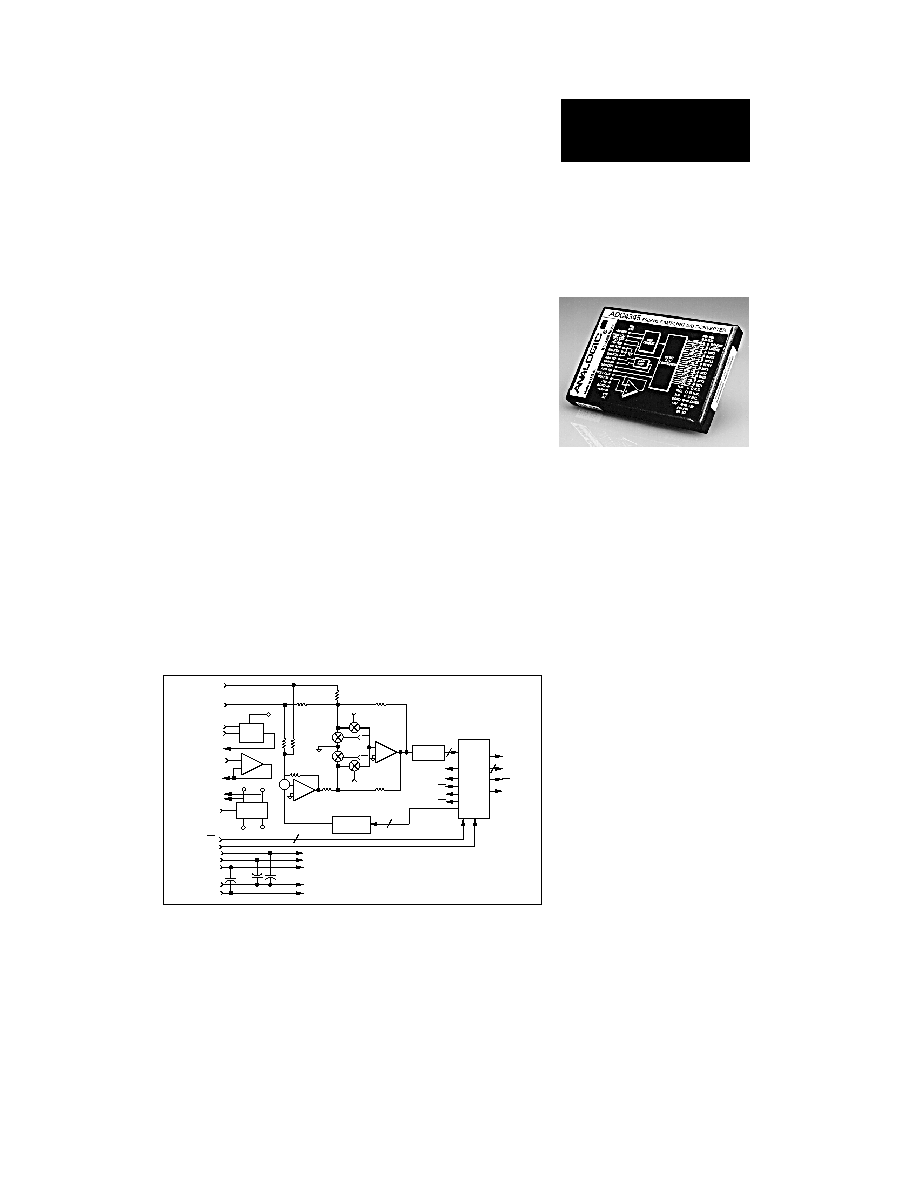
Figure 1. Functional Block Diagram.
S/H
Amp
+
-
+
-
S/H In 1
S/H In 2
S/H Out
S/H
Cont
A/D In
P1
P2
P2
P1
+
-
9
O/U
Flow
B1-B16
Data
En Trig
16
B1
Transfer
S/H Cont
P1
P2
P1
P2
Logic
Ref
Out
Reference
Circuit
+
-
+15V
-15V
Buffer In
Buffer Out
-5V Ref
+5V Ref
Gain Adj
HI & LO
Byte En
Trigger
2
+15V
-15V
+5V
Ana Gnd
Dig Gnd
A/D Offset
Adjust
Summing
Amplifier
RIN
R FB1
Difference
Amplifier
9
RFB
2
9-Bit Flash
ADC
9-Bit DAC
16-Bit Linear
+15V
-15V
+5V
Ana Gnd
Dig Gnd

ANALOG INPUT
Input Voltage Range
Bipolar
±2.5V, ±5V
Unipolar
0 to +10V
Max. Input Without Damage
±15.5V Typ.
S/H Direct Input Resistance
2.5 k
Typ.
Ext. Offset and Gain Adj. Sensitivity
2 mV/V
INPUT BUFFER
2
Input Bias Current
10 nA Max.
Input Resistance
100 M
Typ.
Input Capacitance
10 pF Typ.
F.S. Settling Time
800 ns Typ. to 0.0015%
DIGITAL INPUTS
Compatibility
TTL, HCT, and ACT
Logic "0"
+0.8V Max.
Logic "1"
+2.0V Min.
Trigger
Positive Edge Triggered
Loading
1 TTL Load Min.
Pulse Width
100 ns Min.
High Byte Enable
Active Low, B1-B8, B1
Low Byte Enable
Active Low, B9-B16
INTERNAL REFERENCE
Voltage
±5V, ±0.1% Max
Stability
10 ppm/∞C Max.
Available Current
3
0.5 mA Max.
DIGITAL OUTPUTS
Fan-Out
1 TTL Load
Logic "0"
+0.4V Max.
Logic "1"
+2.4V Min.
Output Coding
Binary, Offset Binary, 2's Comp.
Transfer Pulse
Data valid on positive edge
Over/Under Flow
Valid = logic "0" (occurs only when ±FS
have been exceeded)
DYNAMIC CHARACTERISTICS
4
Maximum Throughput Rate
500 kHz Min. (ADC4345)
1.0 MHz Min. ((ADC4344)
A/D Conversion Time
1.2 µs Typ. (ADC4345)
620 ns Typ. (ADC4344)
S/H Acquisition Time
800 ns Typ. (ADC4345)
380 ns Typ. (ADC4344)
S/H Aperture Delay
15 ns Max.
S/H Aperture Jitter
10 ps rms Max.
S/H Feedthrough
5
≠90 dB Max.; ≠96 dB Typ.
Full Power Bandwidth
1.5 MHz Min. (ADC4345)
3.0 MHz Min. (ADC4344
Small Signal Bandwidth
2.8 MHz Typ. (ADC34345)
4.0 MHz Typ. (ADC34344)
Slew Rate
50V/µs Typ. (ADC4345)
100V/µs Typ. (ADC4344)
Signal to Noise Ratio
6
100 kHz input @ 0 dB
92 dB Min., 95 dB Typ. (ADC4345)
89 dB Min., 92 dB Typ. (ADC4344)
540 kHz input @ -10 dB (ADC4344)
79 dB Min., 82 dB Typ.
Peak Distortion
6
100 kHz input @ 0 dB
≠92 dB Max., ≠99 dB Typ.
@ ≠20 dB
≠92 dB Typ.
540 kHz input @ -10 dB (ADC4344)
84 dB Min., 91 dB Typ.
Total Harmonic Distortion
6
20 kHz input @ 0 dB
≠90 dB Max., ≠97 dB Typ.
@ ≠20 dB
≠82 dB Typ.
100 kHz input @ 0 dB
≠86 dB Max., ≠93 dB Typ. (ADC4345)
≠86 dB Max., ≠97 dB Typ. (ADC4344)
@ ≠20 dB
≠82 dB Typ.
540 kHz input @ -10 dB (ADC4344)
≠79 dB Min., ≠86 dB Typ.
THD + Noise
7
20 kHz input @ 0 dB
89 dB Min., 92 dB Typ. (ADC4345)
87 dB Min., 90 dB Typ. (ADC4344)
@ ≠20 dB
75 dB Typ. (ADC4345)
72 dB Typ. (ADC4344)
100 kHz input @ 0 dB
86 dB Min., 91 dB Typ. (ADC4345)
84 dB Min., 89 dB Typ. (ADC4344)
@ ≠20 dB
75 dB Typ. (ADC4345)
72 dB Typ. (ADC4344)
540 kHz input @ -10 dB (ADC4344)
76 dB Min., 81 dB Typ.
Step Response
8
800 ns Max. to 1 LSB
TRANSFER CHARACTERISTICS
Resolution
16 bits
Quantization Error
±0.5 LSB Max.
Integral Nonlinearity
±0.003% FSR Max.
Differential Nonlinearity
±0.75 LSB Max.
Monotonicity
Guaranteed
No Missing Codes
Guaranteed 0∞C to +60∞C
Offset Error
±0.1% FSR Max. (Adj. to Zero)
Gain Error
±0.1% FSR Max. (Adj. to Zero)
Noise w/o Buffer
9
10V p-p FSR
50 µV rms Typ., 56 µV rms Max.
(ADC4345)
70 µV rms Typ., 80 µV rms Max.
(ADC4344)
5V p-p FSR
35 µV rms Typ., 40 µV rms Max.
(ADC4345)
50 µV rms Typ., 55 µV rms Max.
(ADC4344)
ADC4344/ADC4345
Specifications
1

Noise including Buffer
9
10V p-p FSR
56 µV rms Typ., 70 µV rms Max.
(ADC4345)
79 µV rms Typ., 100 µV rms Max.
(ADC4344)
5V p-p FSR
42 µV rms Typ., 50 µV rms Max.
(ADC4345)
60 µV rms Typ., 70 µV rms Max.
(ADC4344)
STABILITY (0∞C TO 60∞C)
Differential Nonlinearity TC
±1 ppm/∞C Max.
Offset TC
±10 ppm/∞C Max., ±5 ppm/∞C Typ.
Gain TC
±10 ppm/∞C Max., ±5 ppm/∞C Typ.
Warm-Up Time
5 Min. Max.
Supply Rejection per % change
in any supply
Offset
±10 ppm/% Max., ±2 ppm/% Typ.
Gain
±10 ppm/% Max., ±2 ppm/% Typ.
POWER REQUIREMENTS
±15V Supplies
14.55V Min., 15.45V Max.
+5V Supplies
+4.75V Min., +5.25V Max.
+15V Current Drain
100 mA Typ.
≠15V Current Drain
100 mA Typ.
+5V Current Drain
80 mA Typ.
Total Power Consumption
3.4W Typ.
ENVIRONMENTAL & MECHANICAL
Specified Temp. Range
0∞C to 60∞C
Storage Temp. Range
≠25∞C to 80∞C
Relative Humidity
85%, non-condensing to 60∞C
Dimensions
2.5" x 3.5" x 0.44"
(63.5 x 88.9 x 11.18 mm)
Shielding
Electromagnetic 6 sides
Electrostatic 6 sides
Case Potential
Ground
NOTES
1. All specifications guaranteed at 25∞C unless otherwise
noted and supplies at ±15V and +5V.
2. The input buffer need only be used when a high im-
pedance input is required.
3. Reference Load to remain stable during conversion.
4. Dynamic characteristics on ±5V input range and without
input buffer unless otherwise noted.
5. Measured with a full scale step input with a 20V/µs rise
time.
6. See performance testing.
7. THD + noise represents the ratio of the rms value of the
signal to the total RMS noise below the Nyquist plus the
total harmonic distortion up to the 100th harmonic with an
analysis bandwidth of DC to the Nyquist rate.
8. Step response represents the time required to achieve the
specified accuracies after an input full scale step change.
9. Includes noise from S/H and A/D converter.
Specifications subject to change without notice.
Superior performance and ease-of-use of these con-
verters make an ideal solution for those applications
requiring a sample-and-hold amplifier directly at the
input to the A/D converter. Having the S/H amplifier in-
tegrated with the A/D converter benefits the system de-
signer in two ways. First, the S/H is designed specifi-
cally to complement the performance of the A/D con-
verter; for example, the acquisition time, hold mode
settling, and droop rate are optimized for the A/D con-
verter, resulting in exceptional overall performance.
Second, the designer achieves true 16-bit perfor-
mance, avoiding degradation due to ground loops, sig-
nal coupling, jitter, and digital noise introduced when
separate S/H and A/D converters are interconnected.
Furthermore, the accuracy, speed, and quality of the
ADC4344 and ADC4345 are fully ensured by thor-
ough, computer-controlled factory tests of each unit.
SPECIFICATIONS
Input Scaling
The ADC4344 and ADC4345 can be configured for
three input voltage ranges: 0 to +10V, ±2.5V, and ±5V.
The Analog input range should be scaled as close as
possible to the maximum input to utilize the full dynam-
ic range of the converter. Figure 2 describes the input
connections.
Figure 2. Input Scaling Connections.
Pin#
A8
A9
Range
S/H In 1
S/H In 2
0V to +10V
Input
≠5V Ref
±5V
Input
SIG RTN
±2.5V
Input
Input
Continued from page 1.

Coding and Trim Procedure
Figure 4 shows the output coding and trim calibration
voltages of the A/D converter. For two's complement
operation, simply use the available B1 (MSB) instead
of B1 (MSB). Refer to Figure 3 for use of external off-
set and gain trim potentiometers. Voltage DACs with a
±10V output can be utilized easily when digital control
is required. The input sensitivity of the external offset
and gain control pins is 2 mV/V. If the external offset
and gain adjust pins are not used, connect to Pin A12.
To trim the offset of the AD converter, apply the offset
voltage shown in Figure 4 for the appropriate voltage
range. Adjust the offset trim potentiometer such that
the 15 MSBs are "0" and the LSB alternates equally
between "0" and "1" for the unipolar ranges or all 16
bits are in transition for the bipolar ranges.
To trim the gain of the ADC4345, apply the range
(+FS) voltage shown in Figure 4 for the appropriate
range. Adjust the gain trim potentiometer such that the
15 MSBs are "1" and the LSB alternates equally be-
tween "0" and "1".
To check the trim procedure, apply 1/2 full scale volt-
age for a unipolar range or ≠full scale voltage for the
bipolar ranges and check that the digital code is ±1
LSB of the stated code.
Layout Considerations
Because of the high resolution of the ADC4344/
ADC4345 A/D converters, it is necessary to pay care-
ful attention to the printed-circuit layout for the device.
It is, for example, important to return analog and digital
grounds separately to their respective power supplies.
Digital grounds are often noisy or "glitchy", and these
glitches can have adverse effects on the performance
of the ADC4345 if they are introduced to the analog
portions of the A/D converter's circuitry. At 16-bit reso-
lution, the size of the voltage step between one code
transition and the succeeding one for a 5V full scale
range is only 76 µV. It is evident that any noise in the
analog ground return can result in erroneous or miss-
ing codes. It is important in the design of the PC board
to configure a low-impedance ground-plane return on
the printed-circuit board. It is only at this point, where
the analog and digital power returns should be made
common.
PRINCIPLE OF OPERATION
The ADC4344 and ADC4345 are 16-bit sampling A/D
converters with a throughput rate of up to 1 MHz.
These converters are available in two externally config-
ured full scale ranges of 5V p-p and 10V p-p. Both op-
tions are externally or user-programmable for bipolar
and unipolar inputs of ±2.5V, ±5V and 0 to +10V. Two's
complement format can be obtained by utilizing B1 in-
stead of B1.
To understand the operating principles of the A/D con-
verter, refer to the timing diagram of Figure 5 and the
simplified block diagram of Figure 6. The simplified
block diagram illustrates the two successive passes in
the sub-ranging scheme of the AD converter.
The A/D converter section of the converters is factory-
trimmed and optimized to operate with a 10V p-p input
*Gain Adj.
+5V REF
*Off Adj.
Ana Gnd.
≠5V REF
R
1
2
R
1
C
R
1
2
R
1
C
=
=
50K
50K
0.1 µF
=
2
C
2
C
0.1 µF
=
*Note: If not required,
connect to Ana Gnd.
Figure 3. Offset and Gain Adjustment Circuit.
UNIPOLAR BINARY
0V TO +10V
MSB LSB
+FS 111111111111111*
=
+9.99977V
1/2 FS
1000000000000000
=
+5.00000V
Offset
000000000000000*
=
+0.00008V
OFFSET BINARY ±2.5V input
±5V input
MSB
LSB
+FS
111111111111111*
=
+2.49989V
+4.99977V
Offset
****************
=
≠0.00004V
≠0.00008V
+FS
000000000000000*
=
≠2.49996V
≠4.99992V
2'S COMPLEMENT
±2.5V input
±5V input
MSB LSB
+FS
011111111111111*
=
+2.49989V
+4.99977V
Offset
****************
=
≠0.00004V
≠0.00008V
≠FS
100000000000000*
=
≠2.49996V
≠4.99992V
Figure 4. Coding and Trim Calibration Table.
Trigger
S/H Cont
(Internal)
A/D Clock
(Internal)
Transfer
Data
Time (ns)
Hold
Sample
N-1 Data
N Data
0
600 ns
850 ns
1000 ns
25 ns Min.
ADC4344
ADC4345 1.2 µs
1.45 µs
2.0 µs
Figure 5. Timing Diagram.

voltage range. Scaling resistors at the S/H inputs con-
figure the three input ranges and provide a S/H output
voltage to the A/D converter of 10V p-p.
The first pass starts with a low-to-high transition of the
trigger pulse. This signal places the S/H into the Hold
mode and starts the timing logic. At this time, the inter-
nal logic locks out any additional triggers that may in-
advertently occur and corrupt the conversion process
until the routine is complete. The path of the 10V p-p
input signal during the first pass is through a 5:1 atten-
uator circuit to the 9-bit ADC with an input range of 2V
p-p. At 50 ns, the ADC converts the signal and the 9
bits are latched both into the logic as the MSBs and
into the 16-bit accurate DAC for the second pass.
The second pass subtracts the 9-bit, 16-bit accurate
DAC output and the S/H output with the result equal to
the 9-bit quantization error of the DAC, or 19.5 mV p-p.
This "error" voltage is then amplified by a gain of 25.6
and is now 0.5V p-p or 1/4 of the full scale range of the
ADC allowing a 2-bit overlap safety margin. At approxi-
mately 1.2 µs, the DAC and the "error" amplifier have
had sufficient time to settle to 16-bit accuracy and the
amplified "error" voltage is then digitized by the ADC
with the 9-bit second pass result latched into the logic.
At this time the S/H returns to the Sample mode to
begin acquiring the next sample.
The 1/4 full scale range in the second pass produces a
2-bit overlap of the two passes. This is a scheme used
in the A/D converter to provide an output word that is
accurate and linear to 16 bits. This method corrects for
any gain and linearity errors in the amplifying circuitry,
as well as the 9-bit flash A/D converter. Without the
use of this overlapping correction scheme, it would be
necessary that all the components in the A/D converter
be accurate to the 16-bit level. While such a design
might be possible to realize on a laboratory benchtop,
it clearly would be impractical to achieve on a produc-
tion basis. The key to the conversion technique used in
the A/D converter is the 16-bit accurate and 16-bit-lin-
ear D/A converter which serves as the reference ele-
ment for the conversion's second pass. The use of pro-
prietary sub-ranging architecture in the A/D converter
results in a sampling A/D converter that offers un-
precedented speed and transfer characteristics at the
16-bit level.
The ADC4345 has a 3-state output structure. Users
can enable the eight MSBs and B1 with HIBYTEN and
the eight LSBs with LOBYTEN (both are active low).
This feature makes it possible to transfer data from the
A/D converter to an 8-bit microprocessor bus. However,
to prevent the coupling of high frequency noise from the
microprocessor bus into the A/D converter, the output
data must be buffered (see Figure 7).
Figure 7 shows a typical application circuit for the A/D
converter: a four channel, high speed, high resolution
A/D conversion system tied into an 8-bit bus structure.
This circuit could be part of the front end of a medical
imaging system, an ATE system or a sampling oscillo-
scope. The 16-bit resolution provides 96 dB dynamic
range for each channel, and the 500 kHz throughput
rate provides approximately 125 kHz throughput per
channel. (In certain CT imaging applications, it may be
possible to multiplex as many as 24 channels into the
A/D converter.)
For multiplexed inputs, the high input impedance of the
on board buffer input is required. By addressing the
multiplexer at the time of the ADC trigger (Figure 5),
the mux and buffer settling times do not add to the sys-
tem throughput rates.
16-Bit
Linear DAC
≠
+
S/H Amp
A= -1 or -2
S/H In A
S/H In B
S/H Amp
A= -1 or -2
S/H In A
S/H In B
Logic
9
To DAC
(2nd Pass)
2V p-p
10V p-p
10V p-p
±2 mA
DAC In
From
Logic
9
≠
+
≠
+
A= -0.2
A= 6.4
A= 4
0.5V p-p
9
9
16
O/U Flow
B1-B16
EOC
B1
Logic
1st Pass
2nd Pass
9-Bit
ADC
9-Bit
ADC
Figure 6. Operating Principle of the ADC4344 and ADC4345.