Advanced Analog Technology, Inc.
≠
≠
≠
Advanced Analog Technology, Inc
.
≠
Page 1 of 15 V 1.0
AAT1100
Product information presented is current as of publication date. Details are subject to change without notice
TRIPLE-CHANNEL PWM CONTROLLER
Features
Complete PWM Power Control Circuitry
Precision Reference1.25V±1% (25
o
C)
Low Operating Voltage2.5V to 7.0V
Under-Voltage Lockout Protection
Totem Pole Output
Output Short Circuit Protection
Low Dissipation Current
2.5mA at 500 kHz and 50% Duty Cycle
Separate On / Off Control for CH1, CH3 Pair
and CH2 (Refer to Function Table)
Dead Time Control0 to 100%
Wide Operating Frequency50 kHz to 1MHz
Minimized External Components
Pin Configuration
1
2
3
4
5
6
7
8
16
15
14
13
12
11
10
9
IE2
OE 2
OUT2
OUT3
OUT1
SCP
GND
OE3
IE1
IE3
OE 1
OSC
DTC2
DTC13
TOP VIEW
(TSSOP-16 PACKAGE)
DD
V
REF
V
General Description
The AAT1100 provides an integrated triple-channel
pulse-width-modulation (PWM) solution for the
power supply of DC-DC system; this device offers
system engineer the flexibility to custom-make the
power supply circuitry to a specific application.
Each channel contains its own error amplifier,
PWM comparator, dead≠time control (DTC) and
output driver. The under-voltage protection,
oscillator, short circuit protection and voltage
reference circuit are common features of the three
channels.
The AAT1100 contains two boost circuits (CH1,
CH3) and a buck-boost circuit (CH2). DTC can be
set to provide 0% to 100% dead-time through a
divider network. Soft-Start can be implemented by
paralleling the DTC resistor with a capacitor. Two
DTC inputs are assigned for CH1, CH3 pair and
CH2 individually, and DTC inputs can be used to
control on / off operation. In addition, this device
can operate from 2.5V to 7.0V supply voltages to
achieve efficient operation in low power system.
With a minimal number of external components, the
AAT1100 offers a simple and cost effective
solution.

Advanced Analog Technology, Inc.
≠
≠
≠
Advanced Analog Technology, Inc
.
≠
Page 2 of 15 V 1.0
AAT1100
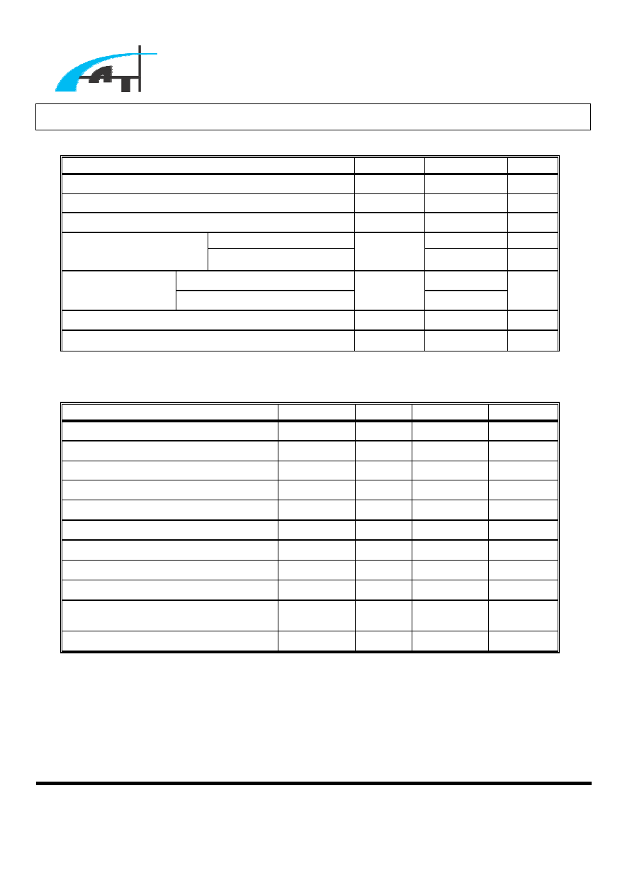
Function Table
Output
Condition
CH1 CH2 CH3
DTC13 > 0.3V, DTC2 > 0.3V
ON "High"
ON "Low"
ON "High"
DTC13 > 0.3V, DTC2 < 0.2V
ON "High"
OFF "High"
ON "High"
DTC13 < 0.2V, DTC2 > 0.3V
OFF "Low"
ON "Low"
OFF "Low"
DTC13 < 0.2V, DTC2 < 0.2V
OFF "Low"
OFF "High"
OFF "Low"
Pin Description
Pin No Name I/O
Description
1
IE2
I Inverting Input Terminal of Error Amplifier 2 (EA2)
2
OE2
I/O Output of Error Amplifier 2 (EA2)
3
DD
V
I Supply
Voltage
4
OUT2
O Channel 2 Output
5
OUT3
O Channel 3 Output
6
OUT1
O Channel 1 Output
7 GND
Ground
8
SCP
I Short Circuit Protection
9
REF
V
O Reference Voltage Output
10
DTC13
I Dead-Time Control of Channel 1, 3 (CH1, CH3)
11
DTC2
I Dead-Time Control of Channel 2 (CH2)
12
OSC
I Frequency Setting Capacitor & Resistor Input
13
OE1
I/O Output of Error Amplifier 1 (EA1)
14
IE1
I Inverting Input Terminal of Error Amplifier 1 (EA1)
15
IE3
I Inverting Input Terminal of Error Amplifier 3 (EA3)
16
OE3
I/O Output of Error Amplifier 3 (EA3)
Advanced Analog Technology, Inc.
≠
≠
≠
Advanced Analog Technology, Inc
.
≠
Page 3 of 15 V 1.0
AAT1100
Absolute Maximum Ratings
Characteristics Symbol
Value
Unit
Supply Voltage
DD
V
8 V
Input Voltage (IE1, IE2, IE3, DTC13, DTC2)
I
V
DD
V
V
Output Voltage
O
V
DD
V
+0.3
V
CH1, CH3
21
41
+
-
/
mA
Output Current
CH2
O
I
41
21
+
-
/
mA
Sink (
w
t
s
2
µ
, Duty10%)
+200
Output Peak Current Source (
w
t
s
2
µ
, Duty10%)
opeak
I
200
-
mA
Operating Temperature Range
C
T
85
to
20
+
-
o
C
Storage Temperature Range
storage
T
125
to
45
+
-
o
C
Recommended Operating Conditions
Symbol
Min
Max
Unit
Supply Voltage,
DD
V
DD
V
2.5 7.0 V
Input Voltage, IE1, IE3
13
I
V
0.95 1.55 V
Input Voltage, IE2
2
I
V
0.4 1.0 V
Output Voltage
O
V
0
DD
V
V
Oscillator (OSC) Capacitance
OSC
C
10 1,800 pF
Oscillator (OSC) Resistance (Note 1)
OSC
R
6 8 k
Oscillator (OSC) Frequency
OSC
f
50 1,000 kHz
Output Current (CH1, CH3)
13
O
I
20
40
+
-
/
mA
Output Current, (CHl, CH2)
2
O
I
40
20
+
-
/
mA
Output Current of Error Amplifier 1, 2
and 3 (EA1, EA1, EA3)
OE
I
60 µA
Operating Temperature
C
T
20
-
85
o
C
Note 1: The rise and fall times of oscillator wave form will be equal at OSC resistor (
OSC
R
) =7 k theoretically.
Advanced Analog Technology, Inc.
≠
≠
≠
Advanced Analog Technology, Inc
.
≠
Page 4 of 15 V 1.0
AAT1100
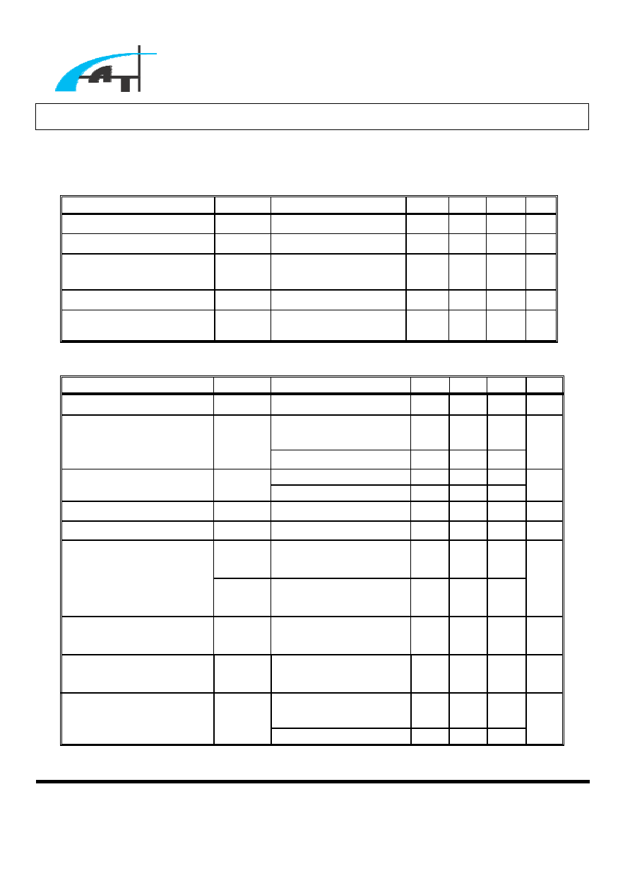
Electrical Characteristics,
3.3V
V
DD
=
;
C
T
= 25
o
C (Unless Otherwise Specified)
Oscillator
Parameter
Test Condition
Min Typ Max
Unit
Oscillator Frequency
OSC
f
OSC
C
= 130pF,
OSC
R
= 7
k
400 500 600
kHz
Oscillator Output Voltage at
High
OSCH
V
OSC
C
= 130pF,
OSC
R
= 7
k
0.95 1.00 1.05 V
Oscillator Output Voltage at
Low
OSCL
V
OSC
C
= 130pF,
OSC
R
= 7
k
0.35 0.40 0.45 V
Frequency Change with
DD
V
V
f
DD
V
= 2.5V to 7V,
OSC
C
= 130pF,
OSC
R
= 7
k
1 2
%
Frequency Change with
Temperature
T
f
(Note 2)
5
10
%
Oscillator Output Current
OSC
I
180
-
200
-
220
-
A
µ
Under-Voltage Protection
Parameter
Test
Condition
Min
Typ
Max
Unit
Upper Threshold Voltage
UPH
V
2.2
2.3
2.4
V
Lower Threshold Voltage
UPL
V
2.0
2.1
2.2
V
Hysteresis (
UPH
V
≠
UPL
V
)
HYS
V
0.1
0.2
0.3
V
Short Circuit Protection Control
Parameter
Test
Condition
Min
Typ
Max
Unit
1
r
V
CH1, CH3
1.10
1.15 1.20
Input Threshold Voltage
2
r
V
CH2 0.20
0.25
0.30
V
Latch Reset Threshold
Voltage
R
V
0.8 1.5 1.8 V
Short Circuit Detect
Threshold Voltage
3
r
V
1.20 1.25 1.30 V
SCP Terminal Source
Current
SCP
I
4
1.
-
0
2.
-
6
2.
-
A
µ
Note 2: The deviation is defined as the difference between the maximum and minimum values obtained over the
recommended temperature range (-20
o
C to 85
o
C).
Advanced Analog Technology, Inc.
≠
≠
≠
Advanced Analog Technology, Inc
.
≠
Page 5 of 15 V 1.0
AAT1100
Electrical Characteristics,
DD
V
= 3.3V;
C
T
= 25
o
C (Unless Otherwise Specified)
(Cont.)
Reference Voltage
Parameter
Test
Conditions
Min
Typ
Max
Unit
Reference Voltage
REF
V
mA
1
I
REF
-
=
1.237 1.250 1.263 V
Short Circuit Output Current
OS
I
=
REF
V
0
2
-
10
-
30
-
mA
Input Voltage Regulation
RI
V
mA
1
I
REF
-
=
,
DD
V
= 2.5V to 7V
2 5
mV
Output Regulation
RO
V
mA
1
.
0
I
REF
-
=
to
mA
1
-
1 5
mV
Reference Voltage Change
with Temperature
R
V mA
1
I
REF
-
=
(Note 3)
15
25
mV
EA (Error Amplifier)
Parameter
Test Condition
Min
Typ Max Unit
Input Offset Voltage
IO
V
CH1,CH3, Unity Gain
15
mV
CH1,CH3,
13
I
V = 0.95V
to 1.55V
±10
±20
Input Bias Current
IB
I
CH2,
2
I
V = 0.4V to 1.0V
±10
±20
nA
CH1, CH3
0.95
1.55
Input Voltage Range
IR
V
CH2 0.4
1.0
V
Open-Loop Voltage Gain
VO
A
OE
R
= 200
k
60 dB
Unity-Gain Bandwidth
1
BW
1
MHz
+
OS
V
V
1
0
V
I
.
+
=
,
A
60
I
O
µ
-
=
1.2
Output Voltage Swing
-
OS
V
V
1
0
V
I
.
-
=
,
mA
2
.
0
I
O
=
0.2
V
Output Sink Current
+
OS
I
V
1
0
V
I
.
-
=
,
V
2
.
0
V
O
=
0.2 1.0 mA
Output Source Current
-
OS
I
V
1
0
V
I
.
+
=
,
V
2
.
1
V
O
=
60
-
100
-
A
µ
CH2, Unity Gain,
C
T = 25
o
C
678
700 722
Input Bias Voltage
5
r
V
CH2, Unity Gain
665
700
735
mV
Note 3: The parameter
R
V is defined as the difference between the maximum and minimum values obtained over the
recommended temperature range (-20
o
C to 85
o
C).