AAT1117
1 Amp Linear Regulator
Advanced Analogic Technologies, Inc.
1250 Oakmead Pkwy, Suite 310, Sunnyvale, CA 94086
(408)524-9684 Fax (408)524-9689
$1$/2*,&
7(&+
TM
1117.2000.05.0.92
General Description
The AAT1117 is a Positive Linear Regulator
designed to deliver 1 amp. It features adjustable
or fixed output voltages and excellent
performance over line and load variations. The
device is able to protect itself and the load from
short circuit conditions with integrated current
limiting circuitry. Thermal shutdown is activated
to prevent damage under extreme conditions.
The AAT1117 is available in surface mount SOT-
223 or TO-252 (DPAK), and through-hole TO-220
packages.
Features
�
Guaranteed 1.2V max Dropout at max current
�
Adjustable or Factory programmed output
voltages
�
Excellent performance over line, load
�
Current
limit
protection
�
Over-Temperature
protection
�
SOT-223, TO-252 (DPAK) and TO-220
packages
Applications
�
Active
SCSI
Terminators
�
High Efficiency Linear Regulators
�
Post Regulators for Switching Supplies
�
Battery
Chargers
�
5V to 3.3V Linear Regulators
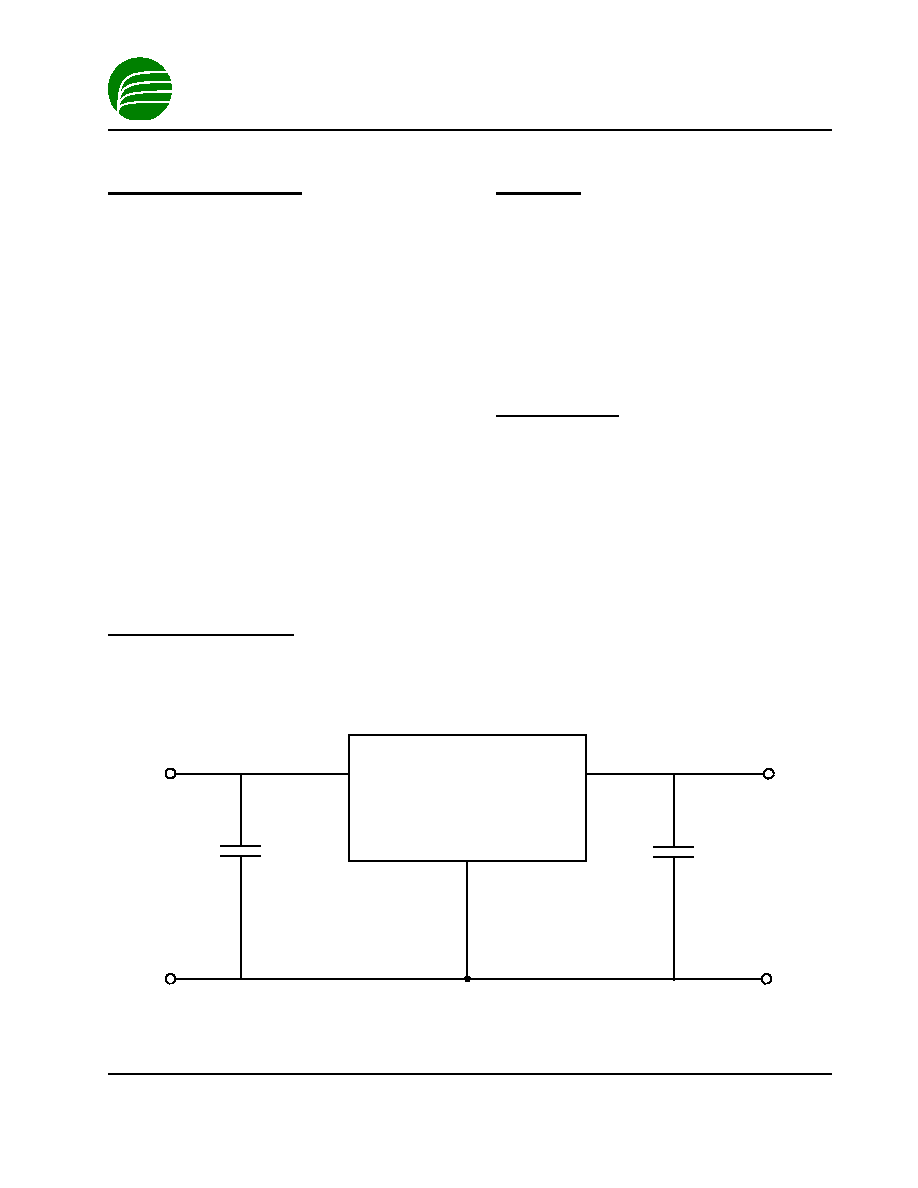
Typical Application
Preliminary Information
2-1
AAT1117
IN
OUT
GND/ADJ
10uF
10uF
INPUT
OUTPUT
AAT1117
1 Amp Linear Regulator
Advanced Analogic Technologies, Inc.
1250 Oakmead Pkwy, Suite 310, Sunnyvale, CA 94086
(408)524-9684 Fax (408)524-9689
$1$/2*,&
7(&+
TM
1117.2000.05.0.92
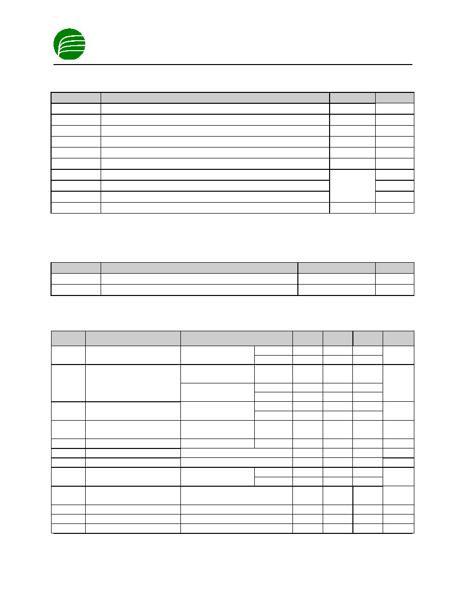
Absolute Maximum Ratings
(T
A
=25
�
C unless otherwise noted)
Symbol
Description
Max
Units
V
IN
Input Voltage
15
V
I
OUT
DC Output Current
P
D
/(V
IN
-V
O
)
mA
T
J
Operating Junction Temperature Range
0 to 125
�
C
JA
Thermal Resistance (SOT-223)
150
�
C/W
JA
Thermal Resistance (TO-252)
80
�
C/W
JA
Thermal Resistance (TO-220)
60
�
C/W
P
D
Maximum Power Dissipation (SOT-223)
mW
P
D
Maximum Power Dissipation (TO-252)
mW
P
D
Maximum Power Dissipation (SOT-220)
Internally
Limited
mW
T
LEAD
Maximum Soldering Temperature (at leads, 10 sec)
300
�
C
Note: Stresses above those listed in Absolute Maximum Ratings may cause permanent damage to the device. Functional operation at
conditions other than the operating conditions specified is not implied. Only one Absolute Maximum rating should be applied at any one
time.
Recommended Operating Conditions
Symbol
Description
Rating
Units
V
IN
Input Voltage
V
OUT
+1.2 to 13.2
V
T
Ambient Temperature Range
-40 to +85
�
C
Electrical Characteristics AAT1117-ADJ
(T
J
=25
�
C unless otherwise noted)
Symbol
Description
Conditions
Min
Typ
Max
Units
T
J
=25
�
C
1.238
1.250
1.262
V
REF
Reference Voltage
V
IN
= 5V, I
OUT
= 10mA
Full temp
1.225
1.250
1.275
V
V
IN
= 4.75 - 7V,
I
OUT
= 10mA
T
J
=25
�
C
0.2
T
J
=25
�
C
0.3
V
OUT
/
V
OUT
Line Regulation
V
IN
= 4.75 - 15V,
I
OUT
= 10mA
Full temp
0.4
%
T
J
=25
�
C
0.05
0.3
V
OUT
/
V
OUT
Load Regulation
V
IN
= 5V,
I
OUT
= 10mA -1A
Full temp
0.2
0.4
%
V
DO
Dropout Voltage
1
I
OUT
= 10mA -1A,
V
OUT
=
�
1%
Full temp
1.0
1.2
V
I
LIM
Current Limit
V
IN
= 2.75 - 7V
Full temp
1.0
A
TC
Ouput Voltage Temp. Coeff.
V
IN
= 2.75 - 7V, I
OUT
= 10mA - 1A
0.005
%/
�
C
V/
T
Temperature Stability
V
IN
= 5V, I
OUT
= 100mA, Full temp
0.5
%
T
J
=25
�
C
55
I
ADJ
Adjust Pin Current
V
IN
= 2.75 - 7V,
I
OUT
= 10mA - 1A
Full temp
90
�
A
I
ADJ
Adjust Pin Current Change
V
IN
= 2.75 - 7V, I
OUT
= 10mA - 1A,
Full temp
0.2
5
�
A
I
OUTMIN
Minimum Load Current
V
IN
= 5V
5
10
mA
V
N
RMS Output Noise
T
J
= 25
�
C
0.003
%V
OUT
PSRR
Ripple Rejection Ratio
V
IN
= 5V, I
OUT
= 1A, Full temp
60
72
dB
2-2

AAT1117
1 Amp Linear Regulator
Advanced Analogic Technologies, Inc.
1250 Oakmead Pkwy, Suite 310, Sunnyvale, CA 94086
(408)524-9684 Fax (408)524-9689
$1$/2*,&
7(&+
TM
1117.2000.05.0.92
Electrical Characteristics AAT1117-3.3 (fixed)
(T
J
=25
�
C unless otherwise noted)
Symbol
Description
Conditions
Min
Typ
Max
Units
T
J
=25
�
C
3.270
3.30
3.330
V
OUT
Output Voltage
V
IN
= 5V, I
OUT
= 0A
Full temp
3.234
3.30
3.336
V
V
IN
= 4.75 - 7V,
I
OUT
= 0A
T
J
=25
�
C
0.2
T
J
=25
�
C
0.3
V
OUT
/
V
OUT
Line Regulation
V
IN
= 4.75 - 15V,
I
OUT
= 0A
Full temp
0.4
%
T
J
=25
�
C
0.05
0.3
V
OUT
/
V
OUT
Load Regulation
V
IN
= 5V,
I
OUT
= 0A -1A
Full temp
0.2
0.4
%
V
DO
Dropout Voltage
1
I
OUT
= 0A -1A,
V
OUT
=
�
1%,
Full temp
1.0
1.2
V
I
LIM
Current Limit
V
IN
= 4.75 - 7V, Full temp
1.0
A
I
Q
Quiescent Current
V
IN
= 5V, I
OUT
= 0-1A, Full temp
6
13
mA
TC
Ouput Voltage Temp. Coeff.
V
IN
= 4.75 - 7V, I
OUT
= 0 - 1A
0.005
%/
�
C
V/
T
Temperature Stability
V
IN
= 5V, I
OUT
= 100mA, Full temp
0.5
%
V
N
RMS Output Noise
T
J
= 25
�
C
0.003
%V
OUT
PSRR
Ripple Rejection Ratio
V
IN
= 5V, I
OUT
= 1A, Full temp
60
72
dB
Note 1: V
DO
is defined as V
IN
- V
OUT
when V
OUT
is 98% of nominal.
2-3
AAT1117
1 Amp Linear Regulator
Advanced Analogic Technologies, Inc.
1250 Oakmead Pkwy, Suite 310, Sunnyvale, CA 94086
(408)524-9684 Fax (408)524-9689
$1$/2*,&
7(&+
TM
1117.2000.05.0.92
Pin Descriptions
Pin #
Symbol
Function
1
GND/ADJ
For the fixed version of AAT1117, pin 1 is the ground connection. For the adjustable
version, this pin is the ADJ pin. See detailed description for further information
regarding configurations.
2
OUT
Output pin � should be decoupled with 10
�
F tantalum or greater output capacitor.
3
IN
Input pin - should be decoupled with 10
�
F tantalum or greater capacitor.
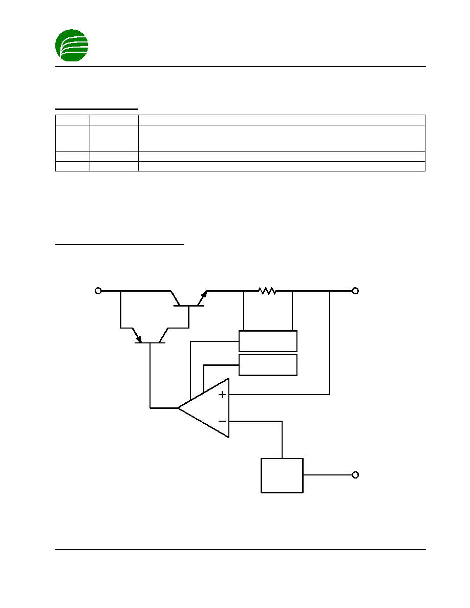
Functional Block Diagram
Over-Current
Protection
Over-Temp
Protection
V
REF
V
IN
GND/ADJ
V
OUT
2-4
AAT1117
1 Amp Linear Regulator
Advanced Analogic Technologies, Inc.
1250 Oakmead Pkwy, Suite 310, Sunnyvale, CA 94086
(408)524-9684 Fax (408)524-9689
$1$/2*,&
7(&+
TM
1117.2000.05.0.92
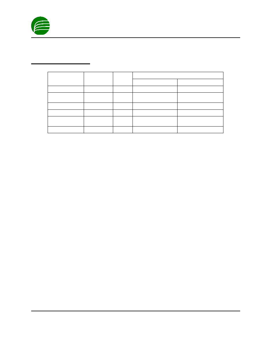
Ordering Information
Part Number
Output Voltage
Package
Marking
Bulk
Tape and Reel
3.3V
SOT-223
AAT1117XMY-3.3-B1
AAT1117XMY-3.3-T1
3.3V
TO-252
(DPAK)
N/A
AAT1117XNY-3.3-T1
3.3V
TO-220
AAT1117XPY-3.3-B1
N/A
Adjustable
SOT-223
AAT1117XMY-ADJ-B1
AAT1117XMY-ADJ-T1
Adjustable
TO-252
(DPAK)
N/A
AAT1117XNY-ADJ-T1
Adjustable
TO-220
AAT1117XPY-ADJ-B1
N/A
2-5