 | –≠–ª–µ–∫—Ç—Ä–æ–Ω–Ω—ã–π –∫–æ–º–ø–æ–Ω–µ–Ω—Ç: AAT1121 | –°–∫–∞—á–∞—Ç—å:  PDF PDF  ZIP ZIP |
AAT1121
1.5MHz, 250mA Step-Down Converter
1121.2006.04.1.0
1
SwitchReg
TM
General Description
The AAT1121 SwitchReg is a member of
AnalogicTech's Total Power Management ICTM
(TPMICTM) product family. It is a 1.5MHz step-
down converter with an input voltage range of
2.7V to 5.5V and output as low as 0.6V. Its low
supply current, small size, and high switching fre-
quency make the AAT1121 the ideal choice for
portable applications.
The AAT1121 delivers 250mA of load current, while
maintaining a low 30A no load quiescent current.
The 1.5MHz switching frequency minimizes the size
of external components, while keeping switching
losses low. The AAT1121 feedback and control
delivers excellent load regulation and transient
response with a small output inductor and capacitor.
The AAT1121 is available in a Pb-free, 8-pin,
2x2mm TDFN package and is rated over the -40∞C
to +85∞C temperature range.
Features
∑
V
IN
Range: 2.7V to 5.5V
∑
V
OUT
Range: 0.6V to V
IN
∑
250mA Max Output Current
∑
Up to 96% Efficiency
∑
30A Typical Quiescent Current
∑
1.5MHz Switching Frequency
∑
Soft-Start Control
∑
Over-Temperature and Current Limit
Protection
∑
100% Duty Cycle Low-Dropout Operation
∑
<1A Shutdown Current
∑
Small External Components
∑
Ultra-Small TDFN22-8 Package
∑
Temperature Range: -40∞C to +85∞C
Applications
∑
BluetoothTM Headsets
∑
Cellular Phones
∑
Digital Cameras
∑
Handheld Instruments
∑
Portable Music Players
∑
USB Devices
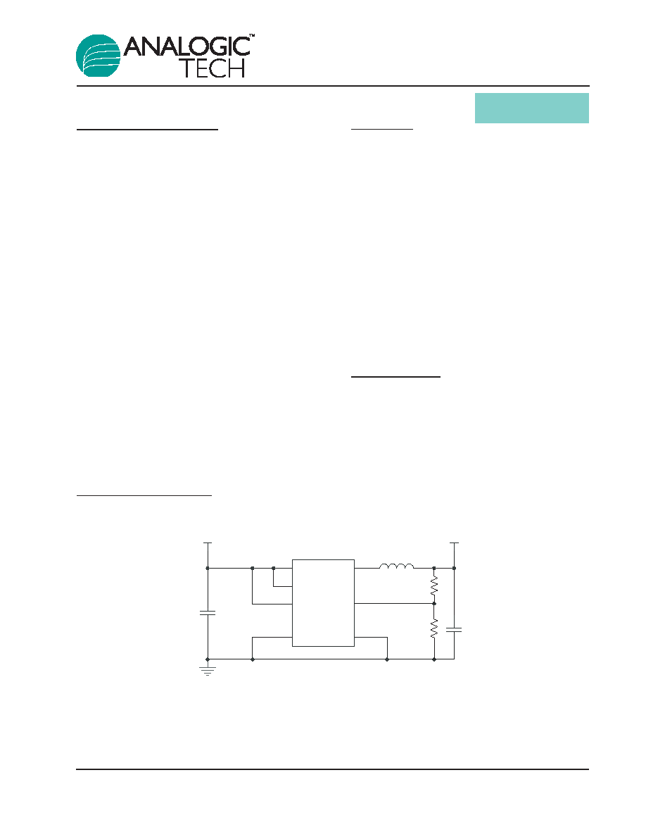
Typical Application
3.0H
L1
R
1
118k
R
2
59k
C
1
4.7µF
C
2
4.7µF
EN
FB
VP
VIN
LX
PGND
GND
AAT1121
V
IN
V
O
= 1.8V 250mA

Pin Descriptions
Pin Configuration
TDFN22-8
(Top View)
GND
FB
VP
VIN
EN
N/C
PGND
LX
3
4
1
2
6
5
8
7
Pin #
Symbol
Function
1
VP
Input power pin; connected to the source of the P-channel MOSFET.
Connect to the input capacitor.
2
VIN
Input bias voltage for the converter.
3
GND
Non-power signal ground pin.
4
FB
Feedback input pin. Connect this pin to an external resistive divider for
adjustable output.
5
N/C
No connect.
6
EN
Enable pin. A logic high enables normal operation. A logic low shuts down
the converter.
7
LX
Switching node. Connect the inductor to this pin. It is connected internally to
the drain of both high- and low-side MOSFETs.
8
PGND
Input power return pin; connected to the source of the N-channel MOSFET.
Connect to the output and input capacitor return.
EP
Exposed paddle (bottom): connect to ground directly beneath the package.
AAT1121
1.5MHz, 250mA Step-Down Converter
2
1121.2006.04.1.0
AAT1121
1.5MHz, 250mA Step-Down Converter
1121.2006.04.1.0
3
Absolute Maximum Ratings
1
Thermal Information
Symbol
Description
Value
Units
P
D
Maximum Power Dissipation
2
W
JA
Thermal Resistance
2
50
∞C/W
Symbol
Description
Value
Units
V
IN
Input Voltage and Bias Power to GND
6.0
V
V
LX
LX to GND
-0.3 to V
IN
+ 0.3
V
V
OUT
FB to GND
-0.3 to V
IN
+ 0.3
V
V
EN
EN to GND
-0.3 to 6.0
V
T
J
Operating Junction Temperature Range
-40 to 150
∞C
T
LEAD
Maximum Soldering Temperature (at leads, 10 sec)
300
∞C
1. Stresses above those listed in Absolute Maximum Ratings may cause permanent damage to the device. Functional operation at condi-
tions other than the operating conditions specified is not implied. Only one Absolute Maximum Rating should be applied at any one time.
2. Mounted on an FR4 board.

Electrical Characteristics
1
V
IN
= 3.6V, T
A
= -40∞C to +85∞C, unless otherwise noted; typical values are T
A
= 25∞C.
Symbol
Description
Conditions
Min
Typ
Max Units
V
IN
Input Voltage
2.7
5.5
V
V
IN
Rising
2.6
V
V
UVLO
UVLO Threshold
Hysteresis
250
mV
V
IN
Falling
2.0
V
V
OUT
Output Voltage Tolerance
2
I
OUT
= 0 to 250mA,
-3.0
3.0
%
V
IN
= 2.7V to 5.5V
V
OUT
Output Voltage Range
0.6
V
IN
V
I
Q
Quiescent Current
No Load
30
A
I
SHDN
Shutdown Current
EN = GND
1.0
A
I
LIM
P-Channel Current Limit
600
mA
R
DS(ON)H
High-Side Switch On Resistance
0.59
R
DS(ON)L
Low-Side Switch On Resistance
0.42
I
LXLEAK
LX Leakage Current
V
IN
= 5.5V, V
LX
= 0 to V
IN
1.0
A
V
Linereg
/
V
IN
Line Regulation
V
IN
= 2.7V to 5.5V
0.2
%/V
V
FB
Feedback Threshold Voltage Accuracy
V
IN
= 3.6V
0.597
0.606
0.615
V
I
FB
FB Leakage Current
V
OUT
= 1.0V
0.2
A
F
OSC
Oscillator Frequency
1.5
MHz
T
S
Startup Time
From Enable to Output
100
s
Regulation
T
SD
Over-Temperature Shutdown Threshold
140
∞C
T
HYS
Over-Temperature Shutdown Hysteresis
15
∞C
V
EN(L)
Enable Threshold Low
0.6
V
V
EN(H)
Enable Threshold High
1.4
V
I
EN
Input Low Current
V
IN
= V
EN
= 5.5V
-1.0
1.0
A
AAT1121
1.5MHz, 250mA Step-Down Converter
4
1121.2006.04.1.0
1. The AAT1121 is guaranteed to meet performance specifications over the -40∞C to +85∞C operating temperature range and is assured
by design, characterization, and correlation with statistical process controls.
2. Output voltage tolerance is independent of feedback resistor network accuracy.
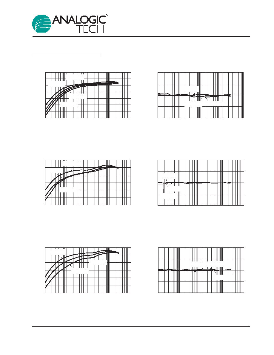
Typical Characteristics
DC Load Regulation
(V
OUT
= 3.0V; L = 4.7µH)
Output Current (mA)
Output Error (%)
-1.0
-0.5
0.0
0.5
1.0
0.1
1
10
100
1000
V
IN
= 5.0V
V
IN
= 4.2V V
IN
= 3.6V
Efficiency vs. Load
(V
OUT
= 3.0V; L = 4.7µH)
Output Current (mA)
Efficiency (%)
40
50
60
70
80
90
100
0.1
1
10
100
1000
V
IN
= 3.6V
V
IN
= 4.2V
V
IN
= 5.0V
DC Load Regulation
(V
OUT
= 1.8V; L = 3.3µH)
Output Current (mA)
Output Error (%)
-1.0
-0.5
0.0
0.5
1.0
0.1
1
10
100
1000
V
IN
= 4.2V
V
IN
= 3.6V
V
IN
= 2.7V
Efficiency vs. Load
(V
OUT
= 1.8V; L = 3.3µH)
Output Current (mA)
Efficiency (%)
40
50
60
70
80
90
100
0.1
1
10
100
1000
V
IN
= 3.6V
V
IN
= 2.7V
V
IN
= 4.2V
DC Load Regulation
(V
OUT
= 1.2V; L = 1.5µH)
Output Current (mA)
Output Error (%)
-1.0
-0.5
0.0
0.5
1.0
0.1
1
10
100
1000
V
IN
= 3.6V
V
IN
= 4.2V
V
IN
= 2.7V
Efficiency vs. Load
(V
OUT
= 1.2V; L = 1.5µH)
Output Current (mA)
Efficiency (%)
30
40
50
60
70
80
90
100
0.1
1
10
100
1000
V
IN
= 3.6V
V
IN
= 2.7V
V
IN
= 5.0V
V
IN
= 4.2V
AAT1121
1.5MHz, 250mA Step-Down Converter
1121.2006.04.1.0
5