SwitchReg
TM
AAT1155
1MHz 2.5A Step-Down DC/DC Converter
1155.2005.11.1.6
1
General Description
The AAT1155 SwitchRegTM is a member of
AnalogicTech's Total Power Management ICTM
(TPMICTM) product family. The step-down switch-
ing converter is ideal for applications where high
efficiency, small size, and low ripple are critical.
Able to deliver 2.5A with an internal power MOS-
FET, the current-mode controlled IC provides high
efficiency. Fully internally compensated, the
AAT1155 simplifies system design and lowers
external parts count.
The AAT1155 is available in a Pb-free MSOP-8
package and is rated over the -40∞C to +85∞C tem-
perature range.
Features
∑
5.5V Max Supply Input
∑
Fixed or Adjustable V
OUT
: 1.0V to 4.2V
∑
2.5A Output Current
∑
Up to 95% Efficiency
∑
Integrated Low On Resistance Power
Switches
∑
Internally Compensated Current Mode Control
∑
1MHz Switching Frequency
∑
Constant PWM Mode
∑
Low Output Ripple With Light Load
∑
Internal Soft Start
∑
Current Limit Protection
∑
Over-Temperature Protection
∑
MSOP-8 Package
∑
-40∞C to +85∞C Temperature Range
Applications
∑
Cable/DSL Modems
∑
Computer Peripherals
∑
High Efficiency Conversion from 5V or 3.3V
Supply
∑
Network Cards
∑
Set-Top Boxes
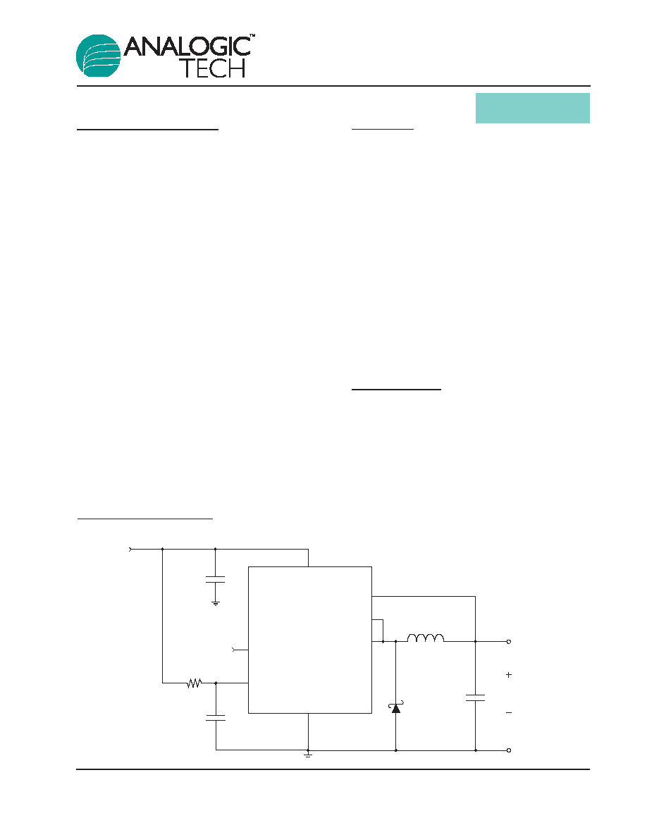
Typical Application
OUTPUT
1.5
µ
H
120
µ
F
LX
LX
VP
FB
GND
AAT1155
VCC
ENABLE
10
µ
F
0.1
µ
F
100
INPUT

AAT1155
1MHz 2.5A Step-Down DC/DC Converter
2
1155.2005.11.1.6
Pin Descriptions
Pin Configuration
MSOP-8
1
2
LX
VP
LX
VP
FB
GND
EN
VCC
1
2
3
4
8
7
6
5
Pin #
Symbol
Function
1
FB
Feedback input pin.
2
GND
Signal ground.
3
EN
Converter enable pin.
4
VCC
Small signal filtered bias supply.
5, 8
VP
Input supply for converter power stage.
6, 7
LX
Inductor connection pin.

AAT1155
1MHz 2.5A Step-Down DC/DC Converter
1155.2005.11.1.6
3
Absolute Maximum Ratings
1
T
A
= 25∞C, unless otherwise noted.
Thermal Characteristics
3
Recommended Operating Conditions
Symbol
Description
Rating
Units
T
Ambient Temperature Range
-40 to +85
∞C
Symbol
Description
Value
Units
JA
Maximum Thermal Resistance
150
∞C/W
P
D
Maximum Power Dissipation
833
mW
Symbol
Description
Value
Units
V
CC
, V
P
V
CC
, V
P
to GND
6
V
V
LX
LX to GND
-0.3 to V
P
+0.3
V
V
FB
FB to GND
-0.3 to V
CC
+0.3
V
V
EN
EN to GND
-0.3 to V
CC
+0.3
V
T
J
Operating Junction Temperature Range
-40 to 150
∞C
T
LEAD
Maximum Soldering Temperature (at leads, 10 sec)
300
∞C
V
ESD
ESD Rating
2
- HBM
3000
V
1. Stresses above those listed in Absolute Maximum Ratings may cause permanent damage to the device. Functional operation at condi-
tions other than the operating conditions specified is not implied. Only one Absolute Maximum Rating should be applied at any one time.
2. Human body model is a 100pF capacitor discharged through a 1.5k
resistor into each pin.
3. Mounted on a demo board (FR4, in still air).
Electrical Characteristics
V
IN
= V
CC
= V
P
= 5V, T
A
= -40∞C to +85∞C, unless otherwise noted. Typical values are T
A
= 25∞C.
Symbol
Description
Conditions
Min Typ Max Units
V
IN
Input Voltage Range
2.7
5.5
V
V
OUT
Output Voltage Tolerance
V
IN
= V
OUT
+ 0.2 to 5.5V,
-2.5
2.5
%
I
OUT
= 0.5A
V
IL
Input Low Voltage
0.6
V
V
IH
Input High Voltage
1.4
V
V
UVLO
Under-Voltage Lockout
V
IN
Rising
2.5
V
V
IN
Falling
1.2
V
UVLO(HYS)
Under-Voltage Lockout Hysteresis
250
mV
I
Q
Quiescent Supply Current
No Load, V
FB
= 0V
630 1000
µA
I
SHDN
Shutdown Current
V
EN
= 0V, V
IN
= 5.5V
1.0
µA
I
LIM
Current Limit
T
A
= 25∞C
4.4
A
R
DS(ON)L
High Side Switch On Resistance
T
A
= 25∞C
60
m
Efficiency
I
OUT
= 1.0A
92
%
V
OUT
(V
OUT
*
V
IN
) Load Regulation
I
LOAD
= 0A to 2.5A
±
2.3
%
V
OUT
/V
OUT
Line Regulation
V
IN
= 2.7V to 5.5V
0.75
%/V
F
OSC
Oscillator Frequency
T
A
= 25∞C
1
MHz
T
SD
Over-Temperature Shutdown
140
∞C
Threshold
T
HYS
Over-Temperature Shutdown
15
∞C
Hysteresis
AAT1155
1MHz 2.5A Step-Down DC/DC Converter
4
1155.2005.11.1.6
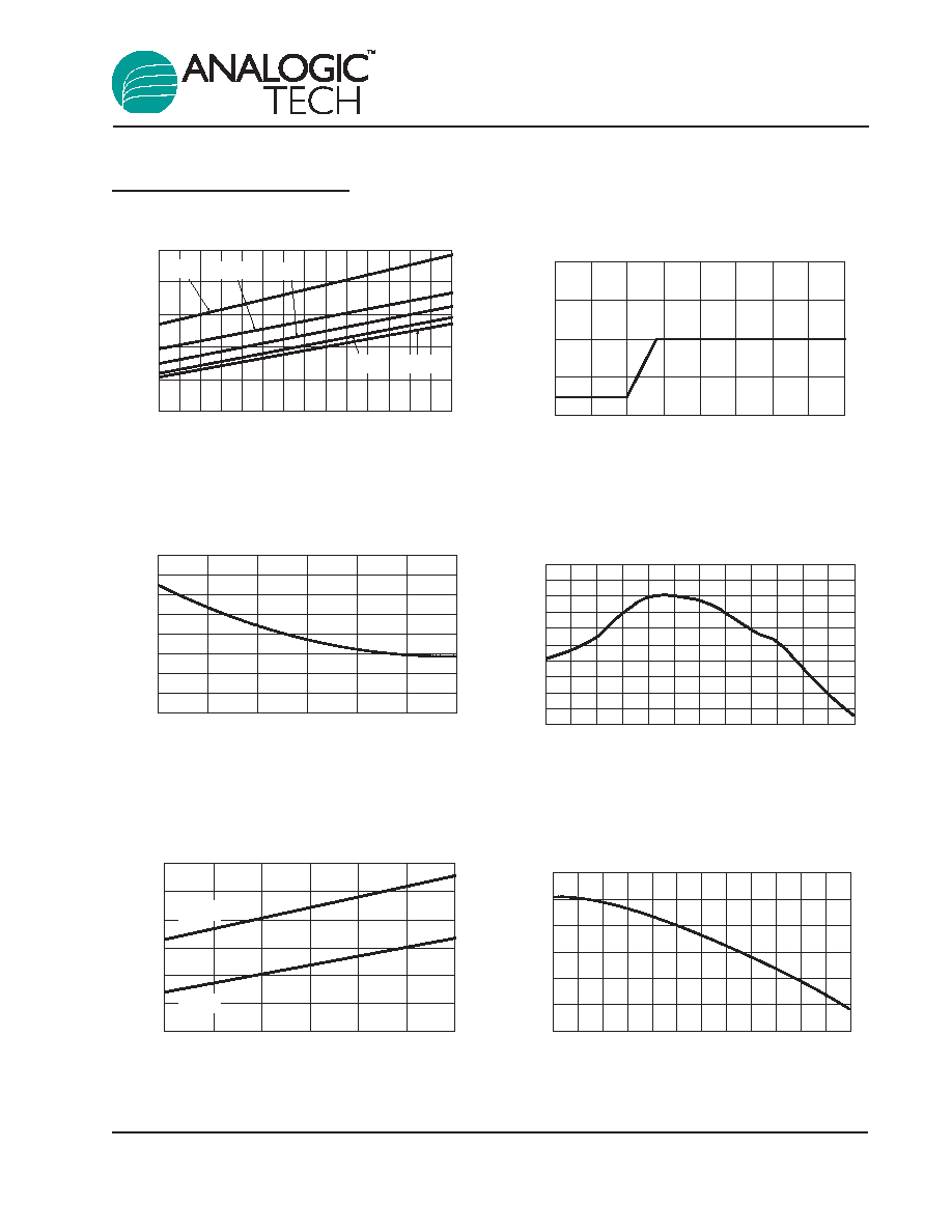
Typical Characteristics
Output Voltage Variation vs. Temperature
(I
OUT
= 2A; V
O
= 3.3V)
-0.8
-0.6
-0.4
-0.2
0
0.2
0.4
-20
0
20
40
60
80
100
Temperature (
∞
∞C)
Variation (%)
Enable Threshold vs. Input Voltage
0.6
0.7
0.8
0.9
1
1.1
1.2
2.5
3
3.5
4
4.5
5
5.5
Input Voltage (V)
Enable Threshold (V)
EN(H)
EN(L)
Oscillator Frequency Variation vs. Temperature
(V
IN
= 5V)
-4
-3
-2
-1
0
1
-20
0
20
40
60
80
100
Temperature (
∞C)
Variation (%)
R
DS(ON)
vs. Input Voltage
(I
DS
= 1A)
40
45
50
55
60
65
70
75
80
2.5
3
3.5
4
4.5
5
5.5
Input Voltage (V)
R
DS(ON)
(m
)
Oscillator Frequency Variation
vs. Input Voltage
(V
OUT
= 3.3V)
-0.5
-0.25
0
0.25
0.5
3.5
4
4.5
5
5.5
Input Voltage (V)
Variation (%)
R
DS(ON)
vs. Temperature
40
50
60
70
80
90
-20
0
20
40
60
80
100
120
Temperature (
∞C)
R
DS(ON)
(m
)
2.7V
3.6V
4.2V
5.0V
5.5V
AAT1155
1MHz 2.5A Step-Down DC/DC Converter
1155.2005.11.1.6
5