General Description
The AAT3119 is a general purpose high efficiency
voltage regulated charge pump IC that can produce
output current levels up to 150mA. As a voltage
regulated output device, it may be used for general
voltage boost applications or to power white, RGB,
or flash type LEDs from a 2.7V to 5.5V input.
The voltage doubling charge pump architecture of
the AAT3119 provides for a low external part count;
just three small ceramic capacitors are needed.
This makes the AAT3119 ideally suited for small
battery-powered applications. This device oper-
ates from a fixed high frequency 1.2MHz oscillator
which enables the use of very small external
capacitors, one 1µF flying capacitor, and two 1µF
bypass capacitors at IN and OUT.
The AAT3119 has built-in soft-start circuitry which
prevents excessive inrush current from the source
supply during startup. A low-current shutdown fea-
ture disconnects the load from V
IN
and reduces
quiescent current to less than 1.0µA when the
device is disabled. The AAT3119 is available in a
Pb-free, 8-pin SC70JW package and is rated over
the -40∞C to +85∞C temperature range.
Features
∑
V
IN
Range: 2.7V to 5.5V
∑
150mA of Output Current
-- Peak Current up to 250mA
∑
Regulated Output Voltage
∑
1.2MHz Switching Frequency
∑
Low Noise Constant Frequency Operation
∑
<1.0µA of Shutdown Current
∑
Automatic Soft Start
∑
Small Application Circuit
∑
Inductorless Boost
∑
8-Pin SC70JW Package
∑
-40∞C to +85∞C Temperature Range
Applications
∑
Cellular Phones
∑
Digital Cameras
∑
Handheld Electronics
∑
PDAs
∑
White LED Backlighting
∑
White LED Camera Flash
AAT3119
High Efficiency 2X Charge Pump
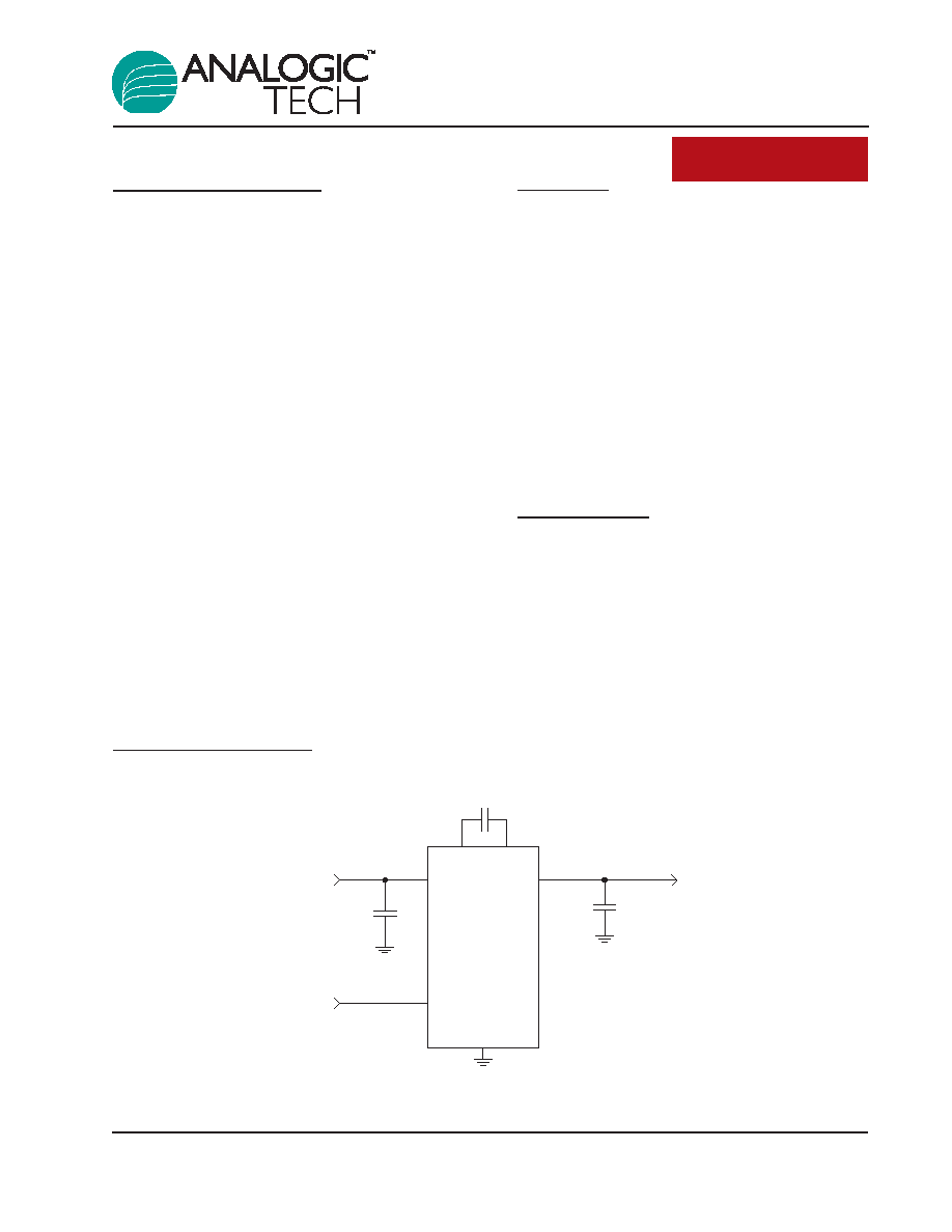
Typical Application
AAT3119
IN
GND
EN
OUT
C
OUT
C
IN
1µF
1µF
1µF
C+
C-
C
FLY
Enable
V
IN
V
OUT
3119.2005.08.1.1
1
ChargePump
TM
Pin Descriptions
Pin Configuration
SC70JW-8
IN
OUT
C+
GND
GND
GND
C-
EN
1
2
3
4
5
6
7
8
Pin #
Symbol
Function
1
EN
Enable input control pin. When low, the device is disabled and consumes
less than 1µA of current. This pin should not be left floating.
2
IN
Input power supply. A 1µF capacitor should be connected between this
pin and ground.
3
OUT
Charge pump output. Connect a 1µF capacitor between this pin and
ground.
4
C+
Flying capacitor positive terminal. Connect a 1µF capacitor between C+
and C-.
5
C-
Flying capacitor negative terminal.
6
GND
Ground connection.
7
GND
Ground connection.
8
GND
Ground connection.
AAT3119
High Efficiency 2X Charge Pump
2
3119.2005.08.1.1
Absolute Maximum Ratings
1
Thermal Information
2
Symbol
Description
Value
Units
JA
Thermal Resistance
160
∞C/W
P
D
Maximum Power Dissipation
3
625
mW
Symbol
Description
Value
Units
V
IN
Input Voltage
-0.3 to 6.0
V
V
OUT
Charge Pump Output
-0.3 to 6.0
V
V
EN
EN to GND Voltage
-0.3 to 6.0
V
V
EN(MAX)
Maximum EN to Input Voltage
0.3
V
I
OUT
Maximum DC Output Current
250
mA
T
J
Operating Junction Temperature Range
-40 to 150
∞C
T
LEAD
Maximum Soldering Temperature (at leads, 10 sec)
300
∞C
AAT3119
High Efficiency 2X Charge Pump
3119.2005.08.1.1
3
1. Stresses above those listed in Absolute Maximum Ratings may cause permanent damage to the device. Functional operation at condi-
tions other than the operating conditions specified is not implied. Only one Absolute Maximum Rating should be applied at any one time.
2. Mounted on an FR4 board.
3. Derate 6.25mW/∞C above 25∞C.

Electrical Characteristics
1
V
IN
= 3.3V; C
IN
= C
OUT
= C
FLY
= 1.0µF; T
A
= -40∞C to 85∞C, unless otherwise noted. Typical values are T
A
= 25∞C.
Symbol
Description
Conditions
Min Typ Max Units
AAT3119-5.0
Power Supply
V
IN
Input Voltage Range
2.7
5.5
V
V
OUT
Output Voltage Tolerance 2.7V < V
IN
< 5V, I
OUT
= 50mA
±4
%
Output Voltage
3.0V < V
IN
< 5V, I
OUT
= 100mA
4.8
5.0
5.2
V
I
CC
Operating Current
V
IN
= 5.0V, Active, No Load Current
2.0
4.5
mA
I
SHDN
Shutdown Current
EN = 0
1.0
µA
I
OUT
Maximum Output Current 3.0 V
IN
5.5
150
mA
Efficiency
V
IN
= 3.0V, I
OUT
= 100mA
82
%
EN
V
EN(L)
Enable Threshold Low
0.4
V
V
EN(H)
Enable Threshold High
EN = 5.5V
1.4
V
I
i
Enable Input Current
-1.0
1.0
µA
Charge Pump
T
SS
Soft-Start Time
200
µs
F
CLK
Clock Frequency
1200
kHz
AAT3119-4.5
Power Supply
V
IN
Input Voltage Range
2.7
5.5
V
V
OUT
2.7V < V
IN
< 5V, I
OUT
= 50mA
±4
%
Output Voltage
3.0V < V
IN
< 5V, I
OUT
= 100mA
4.32 4.5
4.68
V
I
CC
Operating Current
V
IN
= 4.5V, Active, No Load Current
2.0
4.5
mA
I
SHDN
Shutdown Current
EN = 0
1.0
µA
I
OUT
Maximum Output Current 3.0 V
IN
5.5
150
mA
Efficiency
V
IN
= 2.7V, I
OUT
= 100mA
82
%
EN
V
EN(L)
Enable Threshold Low
0.4
V
V
EN(H)
Enable Threshold High
EN = 5.5V
1.4
V
I
i
Enable Input Current
-1.0
1.0
µA
Charge Pump
T
SS
Soft-Start Time
200
µs
F
CLK
Clock Frequency
1200
kHz
AAT3119
High Efficiency 2X Charge Pump
4
3119.2005.08.1.1
1. The AAT3119 is guaranteed to meet performance specifications from 0∞C to 70∞C. Specification over the -40∞C to +85∞C operating
temperature range is assured by design, characterization, and correlation with statistical process controls.
AAT3119
High Efficiency 2X Charge Pump
3119.2005.08.1.1
5
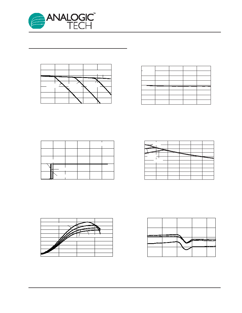
Typical Characteristics _ AAT3119-5V
Oscillator Frequency vs. Supply Voltage
Supply Voltage (V)
Oscillator Frequency (MHz)
1.10
1.15
1.20
1.25
1.30
2.7
3.2
3.7
4.2
4.7
-40∞C
+85∞C
+25∞C
Efficiency vs. Load Current
Load Current (mA)
Efficiency (%)
0
10
20
30
40
50
60
70
80
90
100
0.1
1.0
10
100
1000
V
IN
= 2.7V
V
IN
= 3.0V
V
IN
= 3.3V
V
IN
= 3.6V
Efficiency vs. Supply Voltage
Supply Voltage (V)
Efficiency (%)
0
10
20
30
40
50
60
70
80
90
100
2.7
3.0
3.3
3.6
3.9
4.2
4.5
50mA
100mA
150mA
Supply Current vs. V
EN
V
EN
Control Voltage (V)
Supply Current (mA)
0
1
2
3
4
5
0
1
3
4
2
5
6
I
OUT
= 0µA
V
IN
= 3.3V
V
IN
= 2.8V
V
IN
= 5.5V
Supply Current vs. Supply Voltage
Supply Voltage (V)
Supply Current (mA)
1.00
1.25
1.50
1.75
2.00
2.25
2.50
2.75
3.00
2.5
3.0
3.5
4.0
4.5
5.0
I
OUT
= 0µA
C
FLY
= 1µF
V
EN
= V
IN
Output Voltage vs. Output Current
Output Current (mA)
Output Voltage (V)
4.0
4.2
4.4
4.6
4.8
5.0
5.2
5.4
0
40
80
120
160
200
V
IN
= 2.7
V
IN
= 3.0
V
IN
= 3.3
V
IN
= 3.6